- Products
- Marking
- Alternative
Analog Devices Inc./Maxim Integrated MAX530BCNG+

- Part No.:
- MAX530BCNG+
- Manufacturer:
- Analog Devices Inc./Maxim Integrated
- Category:
- Digital to Analog Converters (DAC)
- Package:
- 24-DIP (0.300", 7.62mm)
- Datasheet:
-
 MAX530BCNG+.pdf
- Description:
- IC DAC 12BIT V-OUT 24DIP
- Quantity:
Unit Price:$0.000000
Ext Price:$0.000000
- Payment:

- Shipping:

Inventory:3
Send us your inquiry,we will respond immediately.
In Stock : 3 PCS
| Qty. | Unit Price | Ext Price |
| 0+ | $0.000000 | $0.000000 |
*Products eligible for online ordering ship within 1-2 business days,please contact us for exact shipping times.
Also you can RFQ for MAX530BCNG+ or email to us: Email: [email protected] , we will contact you within 12 hours.
Product Details
MAX530BCNG+ - Maxim MAX530 +5 V Low-Power 12-Bit Parallel-Input Voltage-Output DAC, Internal 2.048 V Reference, 250 µA, 24-Pin Plastic DIP | MAX530
MAX530BCNG+ is the lead-free 24-pin narrow plastic DIP version of Maxim's MAX530, a +5 V, low-power, 12-bit voltage-output digital-to-analog converter with an on-chip output amplifier and reference. It runs from a single +5 V or dual ±5 V supply, draws only 250 µA (40 µA in shutdown), and includes a buffered output, an internal 2.048 V reference, and a double-buffered parallel interface that talks to 8-bit or 12-bit microprocessors. With 4-quadrant multiplication (no external components), power-on reset and guaranteed monotonicity over temperature, it suits battery-powered data conversion, gain and offset adjustment, industrial process control and automatic test equipment.
Product Introduction
The MAX530 from Maxim Integrated (now part of Analog Devices) is a complete 12-bit voltage-output DAC: the resistor ladder, the output op-amp and a precision reference all live on one chip, so a clean analog voltage appears at VOUT with almost nothing added outside. It is built for low power - 250 µA typical from a single +5 V rail (or ±5 V for bipolar output) - which is why it reaches into battery equipment a hungrier converter cannot. MAX530BCNG+ is the RoHS ("+") option in the 24-pin narrow plastic DIP.
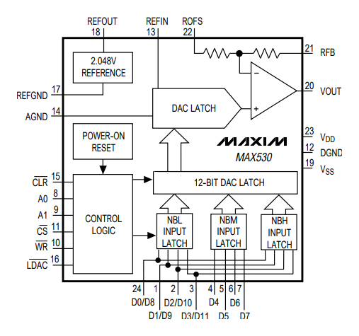
Loading data is flexible. The interface is double-buffered (an input latch followed by a DAC latch), and the 12 bits arrive over a parallel bus organized as three 4-bit nibbles - address lines A0/A1 steer each nibble (low, middle, high) into the input latch, so an 8-bit micro can load the converter in bytes or a 12-bit bus in one pass. A separate LDAC̅ strobe then transfers the input latch to the DAC and updates the output, letting several channels change at once. CS̅ and WR̅ gate the writes; CLR̅ resets the DAC to zero.
The reference and amplifier are designed to be re-used. The on-chip 2.048 V reference appears at REFOUT and is tied to REFIN with a jumper to drive the ladder - or an external reference (DC or AC) can be applied at REFIN instead, which is what makes the part a 4-quadrant multiplying DAC with no external components. The RFB and ROFS pins set the output amplifier's gain and offset (gain of 1 or 2, or bipolar), and REFGND can be tied to VDD to shut the internal reference down and save power. Relative accuracy is ±1 LSB on the B grade, monotonic over the full temperature range, with power-on reset bringing the part up in a known state.
Expert Technical Insight
How is the nibble-loaded DAC driven, and where does the design need care?
- Map the nibbles before you wire the bus: the 12 bits load as three 4-bit groups selected by A0/A1 (see the datasheet's input-latch addressing table). Decide up front whether the host is an 8-bit micro loading bytes or a 12-bit bus loading in one cycle, and route D0-D7 and the A0/A1 lines accordingly - the double-buffered latch then lets you stage data and update on LDAC̅.
- The reference jumper is a real design choice: tie REFOUT to REFIN for the internal 2.048 V and a fixed full scale; drive REFIN externally to multiply - a varying reference at REFIN modulates the output, the basis of 4-quadrant operation. Keep REFGND at AGND when using the internal reference, or to VDD to power it down.
- Single-supply vs bipolar changes the grounds and ROFS: for single +5 V operation tie VSS to AGND; for ±5 V bipolar output use -5 V on VSS and set ROFS for the bipolar offset. Bypass VDD and the REFOUT pin close in, join AGND and DGND at one point, and remember RFB must always connect to VOUT.
Key Benefits
A complete 12-bit DAC that draws just 250 µA (40 µA shut down) from a single +5 V rail - the headline reason it fits battery-powered data conversion.
On-chip output amplifier and 2.048 V reference give a ready buffered voltage at VOUT - minimum external components for the analog system.
A nibble-addressed, double-buffered parallel interface suits 8-bit and 12-bit micros; LDAC̅ updates outputs synchronously across channels.
Drive REFIN externally for 4-quadrant multiplication with no external parts; monotonic over temperature with power-on reset.
Specifications
| Parameter | Value | Condition / Note |
|---|---|---|
| Device Type | 12-Bit Voltage-Output DAC | Parallel input, buffered |
| Manufacturer | Maxim Integrated (Analog Devices) | MAX530 |
| Resolution | 12 bits | |
| Output Type | Voltage (buffered) | On-chip output amplifier |
| Supply | Single +5 V or dual ±5 V | Bipolar output on ±5 V |
| Supply Current | 250 µA (40 µA shutdown) | Low power |
| Reference | Internal 2.048 V | REFOUT; external at REFIN option |
| Interface | Double-buffered parallel | 4-bit nibbles via A0/A1; 8/12-bit µP |
| Multiplying | 4-quadrant | No external components |
| Relative Accuracy | ±1 LSB | B grade (A grade = ±½ LSB) |
| Monotonicity | Guaranteed over temperature | |
| Reset | Power-on reset; CLR̅ to zero | |
| Operating Temperature | 0 to +70 °C | C grade (commercial) |
| Package | 24-Pin Narrow Plastic DIP | Also SO/SSOP; outline 21-0043 |
| Orderable Part Number | MAX530BCNG+ | Pb-free |
Note: Values are taken from the Maxim MAX530 datasheet. Confirm every parameter against the latest official documentation before committing a design.
Package Information
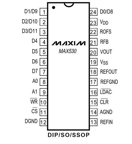
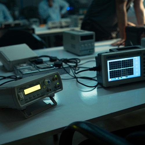
MAX530BCNG+ ships in the 24-pin narrow plastic DIP (0.300-inch body, 0.1-inch pin pitch; package outline 21-0043) - the through-hole package that drops straight into a socket for prototyping, field service and the test-and-measurement gear the part often lives in (the same die is also offered in 24-lead SO and SSOP for surface mount). With only 250 µA flowing there is no thermal concern; layout is about analog cleanliness: bypass VDD and the REFOUT pin close to the package, keep VOUT, RFB and ROFS together at the output amplifier, separate AGND/REFGND from DGND and join them at one point, and route the D0-D7 bus and the CS̅/WR̅/LDAC̅ controls away from the analog pins. The image below shows the 24-lead DIP package.
Pin and Signal Definition
The 24-pin DIP groups the parallel data and control on one side and the analog reference/output on the other (per the MAX530 datasheet):
- Pins 1-7, 24 - D0...D7 (nibble-shared): Parallel data inputs; D0/D8 (pin 24), D1/D9 (1), D2/D10 (2), D3/D11 (3) are nibble-multiplexed, D4-D7 (4-7) complete the bus, addressed by A0/A1.
- Pin 8 - A0, Pin 9 - A1: Address lines selecting the low / middle / high 4-bit nibble into the input latch.
- Pin 10 - WR̅: Write input. Pin 11 - CS̅: Chip select - together load the addressed input latch.
- Pin 15 - CLR̅: Clear - resets the DAC latch to zero. Pin 16 - LDAC̅: Load DAC - transfers input latch to DAC latch and updates VOUT.
- Pin 13 - REFIN: Reference input to the ladder. Pin 18 - REFOUT: 2.048 V reference output (tie to REFIN to use internally).
- Pin 17 - REFGND: Reference ground (to AGND with internal ref, or to VDD to disable it).
- Pin 20 - VOUT: Buffered DAC output. Pin 21 - RFB: Op-amp feedback - always connect to VOUT. Pin 22 - ROFS: Offset resistor - sets gain (VOUT for G=1, AGND for G=2, REFIN for bipolar).
- Pin 23 - VDD: +5 V supply. Pin 19 - VSS: Negative supply (AGND for single-supply, -5 V for bipolar).
- Pin 12 - DGND, Pin 14 - AGND: Digital and analog grounds.
Alternative and Related Parts
The closest options are Maxim's other 12-bit voltage-output DACs - the quad parallel version and several single-channel parts. Match resolution, interface and output configuration to your system before substituting.
| Part Number | Brand | Type / Key Difference | Package | Note |
|---|---|---|---|---|
| MAX527CCNG | Maxim | Quad 12-bit parallel DAC | 24-DIP | Four channels, same bus style |
| MAX5253ACAP | Maxim | Quad 12-bit voltage DAC | 16-QSOP | Serial, +3 V quad |
| MAX5176AEEE+ | Maxim | Single 12-bit voltage DAC | 16-QSOP | Compact single channel |
| MAX5312EAE+ | Maxim | 12-bit voltage DAC, serial | QSOP | Serial-interface alternative |
| MAX5170AEEE | Maxim | 14-bit voltage DAC, serial | 16-QSOP | Higher resolution |
Selection Tips: Stay with the MAX530 when a single-channel 12-bit parallel DAC with on-chip reference and amplifier is wanted in a through-hole DIP; step to the MAX527 for four channels on the same parallel bus. Choose the serial MAX5312/MAX5253 to save pins, the MAX5176 for a compact single channel, or the MAX5170 when 14-bit resolution matters more than the parallel interface.
Manufacturer Information
Maxim Integrated, now part of Analog Devices, Inc. (ADI), built the MAX530 as a "complete" 12-bit DAC for the low-power, minimum-component corner of data conversion - reference, amplifier and double-buffered interface integrated so a microprocessor system gets a clean analog voltage with a jumper and a bypass capacitor.
ADI maintains the datasheet, the input-latch addressing tables and the single-supply versus bipolar application circuits for the part - the guidance that turns the nibble-loaded bus and the REFIN jumper into a working, monotonic 12-bit output on the bench.
Applications

Frequently Asked Questions
How is data loaded into MAX530BCNG+?
Through a double-buffered parallel interface. The 12 bits load as three 4-bit nibbles selected by address lines A0/A1, gated by CS̅ and WR̅ into the input latch; an LDAC̅ strobe then transfers it to the DAC latch and updates VOUT. This suits both 8-bit and 12-bit microprocessors.
Does it have an internal reference?
Yes - an on-chip 2.048 V reference at REFOUT. Tie REFOUT to REFIN to drive the ladder internally, or apply an external reference at REFIN. REFGND can be connected to VDD to disable the internal reference and save power.
Can it do 4-quadrant multiplication?
Yes, with no external components. Driving REFIN with a varying (AC or DC) reference multiplies it by the digital code, and dual ±5 V operation with the ROFS offset pin gives a bipolar output - true 4-quadrant operation.
What supply and power does it need?
A single +5 V supply (or ±5 V for bipolar output), drawing about 250 µA typical and 40 µA in shutdown - low enough for battery-powered equipment. The MAX530BCNG+ is the 24-pin narrow plastic DIP, commercial 0 to +70 °C grade.
Disclaimer
Information Accuracy: The specifications on this page are based on the official Maxim MAX530 datasheet. We work to keep the information accurate and complete, but parameters can change with product revisions, so design engineers should verify all values against the latest official documentation before final design.
Product Authenticity Guarantee: All parts we supply are genuine factory originals with full material traceability.
Technical Support: Pre-sales and post-sales technical consultation is available free of charge.
Application Notice: This page is for reference only. Suitability for a specific application should be confirmed by the design engineer against the actual system requirements.
MAX530BCNG+ Specifications
- Specifications
- Attributes
- Property Value
- Manufacturer
- Analog Devices Inc./Maxim Integrated
- Series:
- -
- Package/Case:
- 24-DIP (0.300", 7.62mm)
- Packaging:
- Tube
- Part Status:
- Active
- Programmable:
- Not Verified
- Number of Bits:
- 12
- Settling Time:
- 25µs (Typ)
- Output Type:
- Voltage - Buffered
- Differential Output:
- No
- Grade:
- -
- Data Interface:
- Parallel
- Reference Type:
- External, Internal
- Number of D/A Converters:
- 1
- Voltage - Supply, Analog:
- ±5V
- Voltage - Supply, Digital:
- 5V
- Mounting Style:
- Through Hole
- INL/DNL (LSB):
- ±1.5 (Max), ±1 (Max)
- Qualification:
- -
- Supplier Device Package:
- 24-PDIP
- Architecture:
- R-2R
- Operating Temperature:
- 0°C ~ 70°C
- Category:
- Digital to Analog Converters (DAC)
MAX530BCNG+ Relevant information
- MAX530BCNG+ Tags
- Popular Search
The following parts are popular search parts in Digital to Analog Converters (DAC).
The Posts
-
Exploring the Features of AN431AN - ATRG1 Voltage Reference IC
The AN431AN - ATRG1 is a significant voltage reference integrated circuit (IC) that plays a crucial role in maintaining stable voltage levels within electronic circuits. Engineered with precision, it o…
-
Unveiling the Wonders of XP1002000 - 05R Electronic Component
The XP1002000 - 05R is an electronic component that stands out for its specialized design and functionality, catering to a variety of electronic system requirements.Unique FeaturesOne of the most notab…
-
Unraveling the Wonders of MMBF170LT1 Transistor
The MMBF170LT1 is a remarkable transistor that has carved a niche for itself in the electronic component landscape. This tiny yet powerful device is engineered with precision to deliver outstanding per…
-
Unveiling the Marvels of MMBF170LT3G Transistor
The MMBF170LT3G is a high - performance transistor that stands out in the realm of electronic components. Engineered with precision, it brings a set of features that make it a valuable asset in numerou…
-
Unveiling the Features of RD16E - T1 - AZ Electronic Component
The RD16E - T1 - AZ is an electronic component that brings a set of unique features to the table. Its design showcases precision engineering, catering to specific requirements in various electronic set…
-
Unveiling the Capabilities of RD16ES - T1 - AZ Electronic Component
The RD16ES - T1 - AZ is a remarkable electronic component that combines advanced technology with practical design to meet the demands of diverse electronic projects.Electrical FeaturesOne of the key as…
Related Products
-
MCP47A1T-A0E/LT
Microchip Technology

-
MCP4706A0T-E/CH
Microchip Technology
-
MCP4716A0T-E/MAY
Microchip Technology
-
MCP4716A0T-E/CH
Microchip Technology
-
MCP4726A0T-E/CH
Microchip Technology
-
MCP4725A0T-E/CH
Microchip Technology
-
MCP4725A1T-E/CH
Microchip Technology
-
MCP4725A2T-E/CH
Microchip Technology
-
MCP4726A1T-E/CH
Microchip Technology
-
MCP4726A3T-E/CH
Microchip Technology
-
MCP4726A2T-E/CH
Microchip Technology
-
MCP4726A0T-E/MAY
Microchip Technology