- Products
- Marking
- Alternative
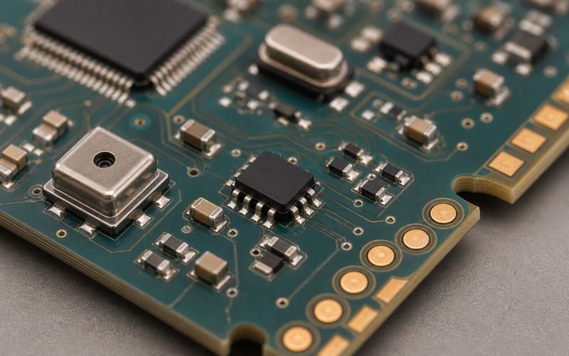
IS25LP128 as Code Storage for Edge AI
IS25LP128 as Code Storage for Edge AI
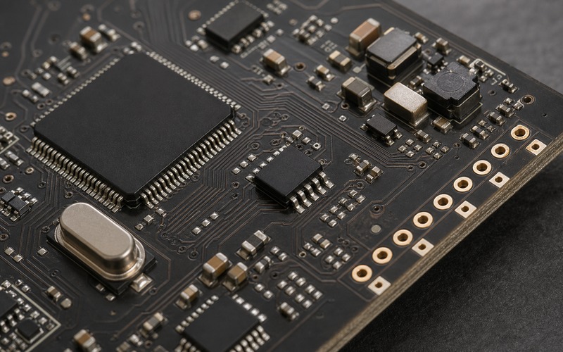
Code storage is easy to overlook on an edge AI board because it does not look like the compute block. The processor, NPU, sensor and power stage get more attention, yet the first executable bytes often come from a small serial NOR Flash. IS25LP128 belongs in that review when a product needs nonvolatile storage for boot code, firmware, model loader, calibration helpers and recovery logic without adding a wide memory bus.
The ISSI data sheet for IS25LP128 identifies it as serial Flash memory and lists different maximum clock ranges across the supply range, including a higher clock class at 2.7V to 3.6V than at 2.3V to 2.7V. That detail is enough to show why the exact voltage rail, suffix, package and controller mode matter. A design should never approve this part by density alone.
Start with the Code That Must Survive Power Loss
Edge AI firmware is more than a boot stub. It may include sensor setup, clock setup, memory controller setup, accelerator drivers, a model loader, preprocessing code, watchdog handling, a field update state machine and a recovery path. Some of that code runs before external RAM is ready. Some runs after a model file is validated. Some is the last path available when a field update fails.
List those code regions before the storage device is approved. The boot region, application region, configuration region, update slot, rollback pointer and factory rescue image should all be named. The flash density can then be checked against the full release layout rather than a small early binary.
Power loss makes the storage plan practical or weak. A device that updates code in the field needs a place to write the new image, verify it and switch state without destroying the image that can still boot. If the storage map leaves no protected state or rescue region, the product may pass lab tests and still be hard to recover.
Keep the Article Focus on Code, Not Model Weight Streaming
IS25LP128 can sit near the same host interface used by model storage parts, but the code-storage review has a different emphasis. A model weight path is judged by sustained reads, burst loading and inference timing. A code path is judged by boot compatibility, executable mapping, update safety, reset behavior and exact command support in the boot ROM or early firmware.
That distinction matters when the design uses execute-in-place. Random instruction fetches, branch-heavy code, interrupt service code and cache line fills can stress the controller in a different way than reading one continuous model file. If critical code executes from serial Flash, test the real code path rather than a bulk read benchmark.
Some products copy code from serial Flash into RAM, then run from RAM. That can reduce runtime dependence on the serial bus, but it shifts attention to copy time, image validation, RAM budget and the failure path if the copy stops midway. The selected storage part still has to work through the exact startup sequence.
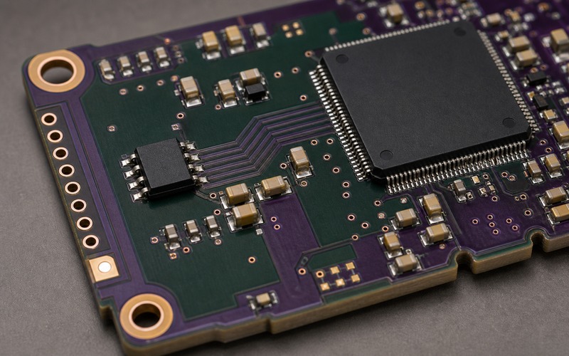
Check Controller Compatibility Before Package Approval
The host controller decides which commands are used, how many data lines are active, how address bytes are sent, how dummy cycles are configured and how status bits are changed. An IS25LP128 orderable suffix can be electrically reasonable and still fail the board if the boot ROM expects another command sequence or a different quad-enable behavior.
Compatibility review should cover single SPI read, faster read modes, dual or quad I/O if used, status register writes, protection bits, erase block sizes, page program limits, suspend behavior, reset support and power-up timing. The part also has to be supported by the production programmer and by any in-circuit recovery method planned for the board.
Use the final processor, final clock rail and final firmware when possible. A flash that works through a desktop programmer is not yet proven as the code source for the product. The pass condition is a clean boot, image validation, firmware update test and controlled recovery after a forced interruption.
Size the Storage Map with Update and Recovery Regions
A 128Mbit class part gives about 16 MB of raw space. The usable layout can be much smaller after alignment, bootloader reserve, application image, factory fallback image, configuration block, metadata, integrity signature and bad-update handling are included. A small edge AI design can consume that space faster than expected once model loader code and hardware abstraction layers are included.
Draw the map as address regions. The first boot path should be clear. The active application should be clear. The region used for a new image during update should be clear. The state that tells the bootloader which image to choose should be protected against half-written values. If a calibration or parameter region shares the same device, its erase block behavior should be reviewed as well.
Erase granularity is a common hidden cost. Updating a tiny state byte can require an erase of a larger block unless the software stores state with a journal or redundant records. If code, parameters and update flags share erase regions carelessly, a simple setting change can place the boot path at risk.
Power and Reset Behavior Need the Same Review as the Data Pins
Serial NOR Flash sits on the edge between power integrity and firmware behavior. The device must wake in a known state, see a valid chip select level, receive stable clocking and hold its contents across the supply range chosen for the board. A weak pull device, noisy rail or bad reset sequence can look like a software problem.
Place decoupling close to the package and keep the return path short. Keep clock and data routes away from noisy switch nodes and high current paths. If the flash shares a rail with radios, motors or an accelerator load step, test boot and read behavior during the real current profile. The board may read cleanly on the bench and fail during a wireless transmit burst or neural accelerator ramp.
The voltage range in the data sheet should be checked against the real rail tolerance, temperature range and startup ramp. A design running near a boundary between clock classes needs margin, not optimism. If the rail is lowered for power saving, verify that the selected read speed and controller setting still fit the lower voltage range.
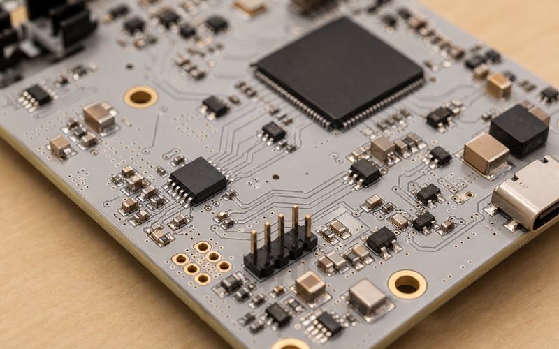
Production Programming Must Be Part of the Layout
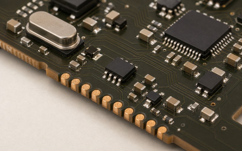
Code storage needs a production path. The board can be programmed before assembly, after assembly through the host, or through direct in-circuit access. Each choice changes test coverage, fixture cost, traceability and failure recovery. A small row of board-edge pads can be the difference between a repairable unit and a board that must be scrapped during launch debugging.
Direct access also helps prove substitutions. If a second-source serial NOR is evaluated, the team can read IDs, program known images, run erase tests and compare boot behavior without depending on an application that may already be failing. That evidence is stronger than a note saying the package and density match.
Production records should capture programmed file identity, flash suffix, package, programmer setting, verification result and board serial reference. Those records make field issues easier to separate: wrong image, wrong storage part, marginal board or firmware defect.
Fixture planning should include both normal programming and recovery programming. A normal path writes the approved release image and verifies it before the unit leaves the line. A recovery path lets engineering take a board that no longer boots, connect through edge pads and read enough flash state to learn what happened. If both paths use the same pads, access rules, pad finish, keepout and probe pressure should be checked during layout review. If the recovery path uses the host processor, the team should confirm that the processor can still reach the flash when the application image is empty, corrupted or protected. This is a practical test point decision as much as a memory selection decision.
Substitution Risk Is Software Risk
Many serial NOR devices share a familiar footprint, but replacements are not approved by footprint and density alone. Differences in command set details, status register layout, quad-enable bit location, protection defaults, reset command, unique ID length, erase timing, program timing and deep power-down behavior can affect boot and update behavior.
For IS25LP128, treat each proposed alternate as a software-facing component. The alternate should run through cold boot, warm reset, low-voltage start, update, interrupted update, image verification, power-down wake and recovery programming. A part that reads through a programmer but needs a firmware change is not a drop-in replacement for a released board.
Package review also matters. Pad size, body height, moisture handling, assembly profile and inspection access affect manufacturing. A board built for one footprint can accept an alternate electrically yet create solder yield or rework issues if the exact package is not controlled.
Security and Integrity Belong in the Storage Plan
Code storage should carry an identity check. At minimum, the bootloader needs image length, version, region information and an integrity check before it jumps into application code. Some products need signatures, anti-rollback rules or a secure update policy. The flash selection cannot define that policy, but it must leave room and access behavior for it.
Do not mix debug convenience with release policy. A board may need service access during development and protected behavior in the field. Decide which pads remain reachable, which commands are disabled by firmware policy, and which region can be rewritten during normal service. The answer depends on product risk, but it should be decided before the storage map is frozen.
Integrity checks should be exercised in test. A fixture that writes and reads bytes is useful, yet it does not prove the product will reject a damaged image. Add a controlled bad-image case during engineering validation so the recovery path is known before production.
Final IS25LP128 Selection Checklist
Before approving IS25LP128 for edge AI code storage, confirm the exact orderable suffix, voltage rail, read speed at that rail, package, host controller command mode, boot ROM support, execute-in-place or copy-to-RAM strategy, storage map, update slots, recovery image, integrity method, erase granularity, power ramp, decoupling, route length, production programming access and qualified alternate list.
The part is a good fit when the code path is predictable, the storage map survives failed updates, production can program and verify the image, and every alternate has passed the same boot and update tests. It is a risky fit when the team treats serial NOR as a generic memory footprint and leaves boot, update, voltage and substitution proof until the board is already late.