- Products
- Marking
- Alternative
W25Q128JV Holding the Boot Image and Model on an Edge Device
W25Q128JV Holding the Boot Image and Model on an Edge Device
A model can fit in flash and still fail the product review if the boot path is treated as a loose storage choice. W25Q128JV sits in the class of Winbond serial NOR flash used for code storage, so the first question is not how large the device looks on a distributor line. The first question is what the board expects this memory to do when power rises, firmware starts, and a model image has to be found without guesswork.
In many edge devices, this part is the nonvolatile place where a boot image, firmware payload, model file, calibration table or parameter set can live. It is usually not the fast working memory that carries every activation during inference. Keeping that boundary clear prevents a common design mistake: approving a flash footprint as if it can replace SRAM, SDRAM or LPDDR in the live data path.
Define the Storage Role First
The storage role should be written in plain board terms. Is W25Q128JV holding a first-stage bootloader, a complete application image, a model binary, a rollback image, calibration data, a device certificate, a field log, or a mix of those items? The answer changes the approval checks. A boot image cares about first-read reliability and controller support. A model file cares about size, update process, read pattern and integrity check. A log cares about erase behavior and wear management.
Keep the role separate from the memory family name. Serial NOR flash gives compact nonvolatile storage through a small pin count interface, but the board still has to decide whether the host copies data into RAM, executes in place through a cache, or reads selected blocks on demand. The same part can be acceptable in one role and weak in another.
A useful release record names each stored item, its expected size, the owner firmware, the update route and the validation method used at production test. That record is what later keeps a purchasing change from becoming a firmware fault.
Read W25Q128JV as a Full Orderable Part
The base name points the engineer toward the memory family, but the full orderable string controls package, suffix, temperature range, voltage family, reel option and sometimes behavior that the boot code depends on. W25Q128JV should be reviewed with the exact suffix used on the approved BOM. A shortened purchasing note can land on a package or grade that fits a spreadsheet but not the board.
The common engineering shorthand also hides density math. A 128 Mbit serial NOR class device gives about 16 MB of raw storage before file system, headers, partitions, redundancy or image signing overhead are counted. A model that is 13 MB in a lab folder may not fit after version metadata, fail-safe image space or bootloader reserve area is added. Capacity approval needs the partition plan, not the model file size alone.
Package review belongs in the same step. A small 8 pin package can look harmless, yet land pattern, body width, height, solder fillet visibility and assembly inspection can differ between suffixes. The approved drawing and the chosen manufacturing process have to agree.
Separate Boot Flash from Working Memory
Boot flash is the nonvolatile source. Working memory is where the processor, accelerator or DSP keeps live code, stacks, buffers, tensors and temporary results. The two roles may touch during startup, but they are not interchangeable. A board can load weights from W25Q128JV at boot, then run inference from internal SRAM or external DRAM. Another design may execute code directly from flash through a QSPI controller and cache. Those are different performance and failure cases.
If the product relies on execute in place, review cache size, miss penalty, controller mode, clock, bus width and firmware alignment. If the product copies the image to RAM, review transfer time, brownout behavior, image verification and what happens when the copy is interrupted. If the product reads model blocks from flash during inference, review access locality and latency, because random reads can slow a pipeline that looked fine during a sequential file copy.
Do not approve the part by saying it is enough memory. Approve it by proving how the data moves from nonvolatile storage into the place where the edge device runs.
Check the Host Interface and Boot Mode
W25Q128JV is used in systems that expect serial NOR behavior through SPI, Dual SPI, Quad SPI or related controller modes, depending on host support and exact setup. The host has to support the command set and mode used by the boot ROM or firmware. A board that can speak ordinary SPI after firmware starts may still fail if the boot ROM expects a specific quad-read mode, dummy cycle setting, address length or status bit state.
The boot process should be written as a sequence: power rails valid, reset released, clock stable, chip select state valid, first command issued, image header checked, image copied or mapped, then application handoff. Each step gives a place to test and a place for an alternate flash to fail.
Pull resistors, chip select routing and reset or hold pins should not be left for the layout review alone. The logic state at power transition decides whether the host can see the flash at the first attempt.
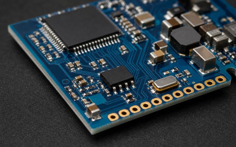
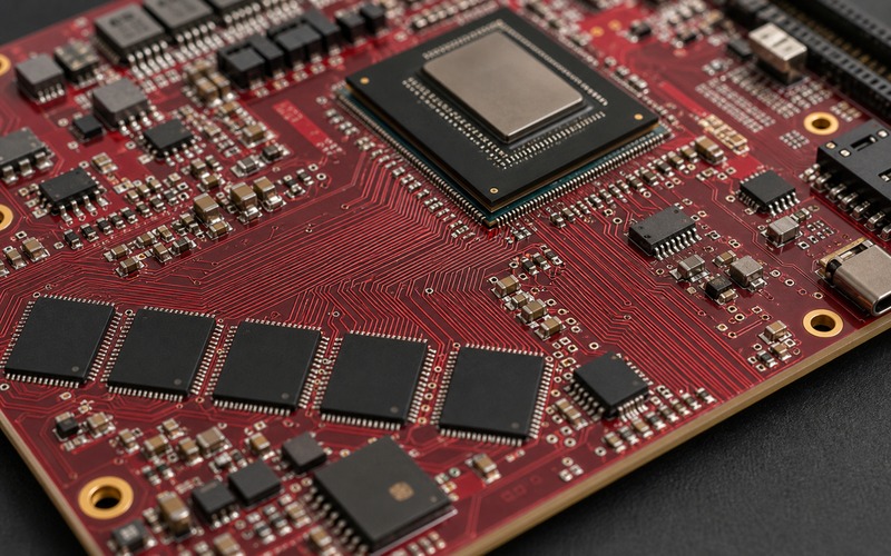
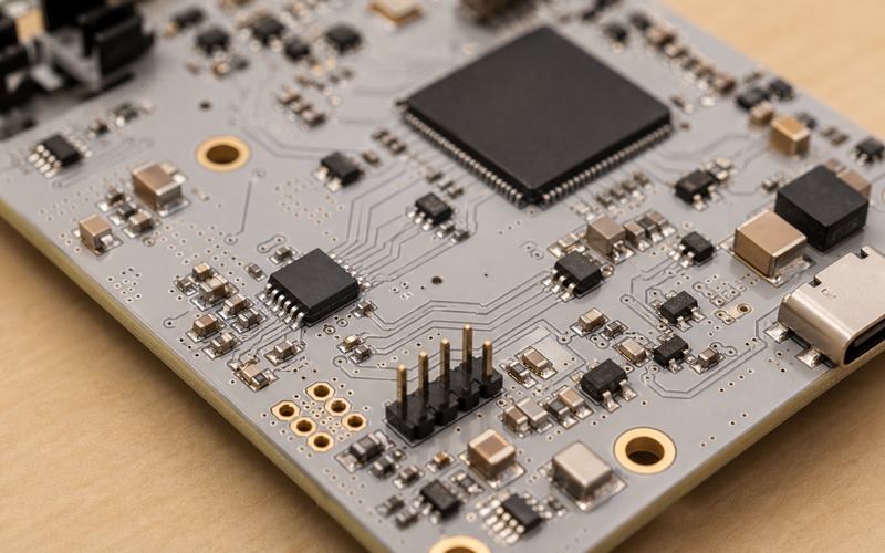
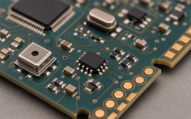
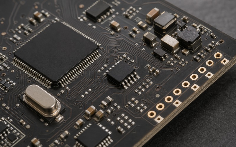
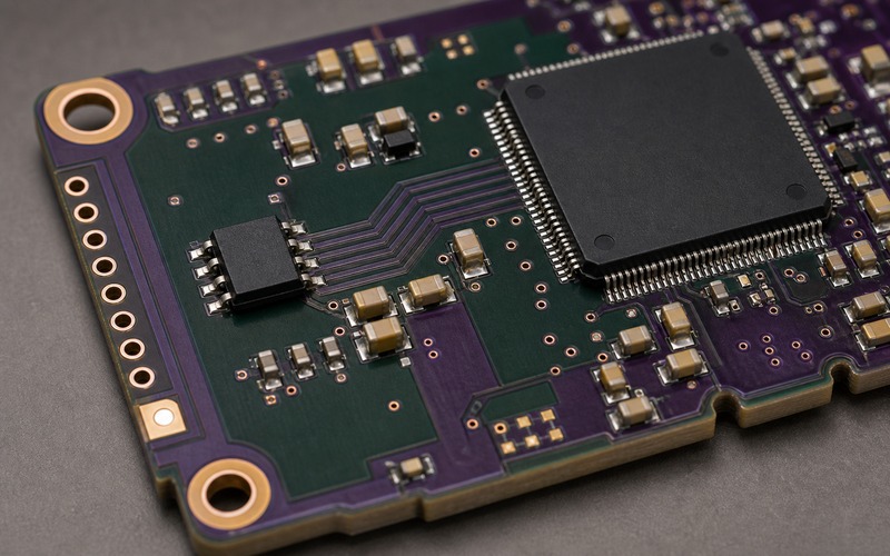
Layout Makes the Boot Path Visible
The memory should sit close to the host that reads it, with a clean route for clock, chip select and data pins. The path is narrower than a DDR bus, yet it still needs a return path, decoupling, pin access and enough spacing from noisy switching nodes. A noisy clock line, weak decoupling or long route around a connector can turn the boot path into a temperature or power-cycle problem.
Place the service features where production can reach them. Programming pads, a board edge access row or a pogo fixture area helps the factory load, verify or recover units. Hiding these pads under a heat spreader, cable or tall component makes every service case harder to repair. The inline board view follows this rule by keeping the pads along the board edge and the flash close to the host.
The layout record should also name the parts around the memory: decoupling capacitors, series damping if used, pull devices and the oscillator or host clock context. These small components often explain boot failures faster than the large processor does.
Plan the Image Format and Update Path
A production image is more than a binary file. It usually needs a header, version field, length field, checksum or signature, rollback decision, protected bootloader area and perhaps a model version tied to application firmware. If the flash also stores calibration values, the erase blocks and update process must protect those values when firmware changes.
For field update, decide whether the product writes a new image into unused space, verifies it, switches a boot flag and keeps the old image for recovery. If there is no room for that method, the update plan may require a different density or a different memory layout. If the product is factory programmed only, the process still needs a read-back or functional check that proves the image loaded on the part matches the release file.
Keep the model file tied to firmware. A model built for one preprocessing path or tensor layout can be wrong even when the flash programming step is correct. The release record should carry model version, firmware version and flash layout together.
Integrity Checks Are Part of Storage Selection
Boot storage is judged by recovery behavior as much as by successful startup on the bench. Check what the device does when power drops during programming, when the first image header is damaged, when a block erase is interrupted, or when an update package is rejected. A design with no integrity check may boot in the lab and fail during a customer update.
The storage plan should include at least one way to reject a wrong or damaged image before execution. That can be a checksum, signature, version rule or a host-specific secure boot process. The exact method belongs to the system design, yet the flash choice must leave enough space and access behavior for that method to work.
For products with field service risk, recovery access matters. A board that has pads or a connector near the flash gives engineering a way to recover units and investigate image faults without replacing the processor.
Erase and Program Behavior Changes Firmware Design
Serial NOR flash is read often and erased in blocks. Firmware should not rewrite small parameters as if it were writing RAM. Parameters, counters and logs need an erase-aware format, wear distribution if they change often, and a clear rule for preserving calibration data during firmware update.
Model files are larger and usually change less often, but they still need a plan. A large erase block can force the update code to move or protect nearby data. A file system can help, yet it adds overhead, metadata and failure modes. A raw partition can be compact, yet it places more responsibility on the firmware.
The part selection review should name which regions are read-only after programming, which regions can be updated, and which regions must survive a failed update. That is a storage map, not a marketing capacity claim.
Power and Timing Need Startup Evidence
Flash current is modest compared with a large processor, but startup timing still depends on valid supply, reset and host clock. A board should be tested with the final regulator ramp, final pull devices and final firmware. Slow bench supplies and debug probes can hide first-boot timing problems that appear later in a sealed product.
Measure startup across the product temperature and voltage range that the design claims. The evidence does not need to be elaborate, but it should prove that the host can read the flash, verify the image and enter the application state without repeated resets. If the device wakes from a low-power state, test that path as well. Wake-and-read behavior can differ from a cold boot.
Keep the boot log tied to board revision. A change in regulator, oscillator, pull resistor or flash suffix can alter startup margin even when the schematic still looks close.
Substitution Is a Command and Process Question
A replacement serial NOR flash has to match the board and the software. Density, voltage, package, pinout, temperature grade, read modes, command set, status register behavior, quad-enable handling, erase geometry, program timing, protection bits, unique ID behavior and programmer support all matter. A part can share a footprint and still break boot because the ROM loader reads a status bit differently.
Do not let the purchasing substitute be defined as any 128 Mbit SPI flash. Write approved alternates by exact part, package and tested boot mode. If the alternate needs a firmware setting, a new boot command table or a different programmer profile, that requirement belongs in the approval note.
For a product expected to live for years, the substitute plan should also name the test used to qualify the replacement: cold boot, warm reset, image update, rollback check, production programming and a short inference load that proves the model was read and accepted.
Production Programming and Inspection
Factory programming can happen before placement, after assembly or both. Each route needs a controlled file, programming tool version, adapter or fixture, checksum record and label or traceability rule. If the part is programmed after assembly, the access pads or connector should be reachable without stressing nearby components.
Inspection should verify orientation, package, solder joints, decoupling population, pull devices and accessible programming path. A blank flash, wrong image, damaged pad, wrong suffix or missing capacitor can look like a processor failure until the boot path is checked in order.
Production test should avoid a weak pass condition. Seeing a logo, prompt or LED blink may prove boot, but it may not prove that the correct model file was read. A stronger test asks the firmware to report image version, model version and a known inference or checksum result.
Final W25Q128JV Review Checklist
Before approving W25Q128JV for an edge device, confirm the exact suffix, package, voltage family, host controller mode, boot ROM requirements, storage map, model size, image integrity method, update path, erase behavior, layout placement, decoupling, programming access, production verification and approved alternates. Keep body links out of the article until the target product or article page has been checked live and returns a stable page.
The part is a good fit when it makes the boot image and model storage predictable, testable and recoverable. It is a risky fit when the team treats the flash as a generic memory bucket and leaves boot mode, update behavior and alternate approval for the last production week.
Related information
- 2026.07.01 IS25LP128 as Code Storage for Edge AI
- 2026.07.01 MT25QL128 Feeding Weights Over QSPI