 Free Shipping Over$200

- Products
- Marking
- Alternative

Texas Instruments LM5140QRWGRQ1

- Part No.:
- LM5140QRWGRQ1
- Manufacturer:
- Texas Instruments
- Category:
- DC DC Switching Controllers
- Package:
- 40-VFQFN Exposed Pad
- Datasheet:
-
 LM5140QRWGRQ1.pdf
- Description:
- DUAL SYNCHRONOUS BUCK CONTROLLER
- Quantity:
Unit Price:$0.000000
Ext Price:$0.000000
- Payment:

- Shipping:

Inventory:2,492
Send us your inquiry,we will respond immediately.
In Stock : 2,492 PCS
| Qty. | Unit Price | Ext Price |
| 0+ | $0.000000 | $0.000000 |
*Products eligible for online ordering ship within 1-2 business days,please contact us for exact shipping times.
Also you can RFQ for LM5140QRWGRQ1 or email to us: Email: [email protected] , we will contact you within 12 hours.
Product Details
LM5140QRWGRQ1 - TI Wide-Input Dual-Channel Synchronous Buck Controller, 3.8V to 65V, 2.2MHz, AEC-Q100, VQFN-40 | LM5140-Q1
LM5140QRWGRQ1 is the tape-and-reel, AEC-Q100 qualified orderable version of Texas Instruments' LM5140-Q1, a dual-channel synchronous buck controller that drives the external high-side and low-side MOSFETs of two independent step-down regulators from a wide 3.8 V to 65 V input (70 V absolute maximum). The two channels run 180° interleaved to halve input ripple, each regulating a ±1% output that is pin-selectable to fixed 3.3 V / 5 V (channel 1) or 5 V / 9 V (channel 2), or adjustable from 1.5 V to 15 V, switching at a selectable 2.2 MHz or 440 kHz. With split high-side/low-side gate-drive outputs for dead-time control, programmable current limit, independent enables and power-good flags, and a 9 uA shutdown, it targets automotive infotainment, instrument-cluster, body and ADAS power rails in a 40-pin VQFN with wettable flanks.
Product Introduction
LM5140-Q1 is a controller, not an integrated converter: it supplies the loop control, gate drive and protection for two synchronous buck power stages while the power MOSFETs and inductors sit outside the package. That split is what lets one small VQFN regulate rails that draw far more current than any integrated-FET device could, because the designer picks the external FETs to match the load. Each of the two channels is a complete current-mode buck controller with its own soft-start, feedback, compensation, current sense, enable and power-good, so the part behaves like two independent regulators that happen to share one bias supply and one oscillator.
The wide 3.8 V to 65 V input is the reason the device is aimed at automotive: it rides through cold-crank dips toward 3.8 V and load-dump transients toward the 70 V absolute maximum without the pre-regulator a narrower-input controller would need. The two channels are clocked 180 degrees out of phase, so their input current pulses interleave and the RMS ripple the input capacitors must absorb drops sharply, shrinking the input filter. Each output is accurate to within 1% and can be set by pin-strap to common fixed rails or divided down with a resistor pair anywhere from 1.5 V to 15 V, and the switching frequency is a simple choice between 2.2 MHz for the smallest magnetics and 440 kHz for the highest efficiency, with an OSC pin and SYNC input for anything in between.
Where LM5140-Q1 earns its place is drive flexibility and protection. The high-side and low-side gate drivers each break out separate turn-on and turn-off pins (HO/HOL and LO/LOL), so a designer tunes the rise and fall edges and the dead time independently to trade switching loss against shoot-through margin. Current limit is programmed by a single resistor and uses low-side MOSFET sensing, an emulated peak-current scheme keeps it stable at high duty cycles, and a sustained overload folds the part into hiccup mode rather than letting the FETs cook. A SYNC output lets a second LM5140-Q1 or downstream converter lock to the same clock for a clean multi-rail board.
Expert Technical Insight
What does a controller-plus-external-FET architecture buy a designer over an integrated-FET module, and what does it ask in return?
- Current scales with the FETs, not the chip: Because LM5140-Q1 only drives the switches, the same controller serves a 2 A camera rail and a 15 A processor rail simply by changing the external MOSFETs and inductor. An integrated-FET part caps out at its on-chip silicon; here the power path is the designer's to size.
- Split gate drive is a tuning tool, not a complication: Separate HO/HOL and LO/LOL pins let you slow the turn-on edge with one resistor to cut EMI while keeping turn-off fast for efficiency, and set dead time by design rather than accepting a fixed internal value. In a noise-sensitive cluster or infotainment board this is often the difference between passing and failing CISPR 25.
- Plan the bias and the layout up front: The split needs an external bias rail (VCC/VCCX) and tight gate-loop layout for HO/SW/HB and LO/PGND; current-sense and compensation are external too. The reward is a rugged, accurate, automotive-grade two-rail supply, but the loop and the gate loops are the engineer's responsibility, not the chip's.
Key Benefits
A wide input that survives cold-crank down toward 3.8 V and load-dump up to a 70 V absolute maximum, so both rails stay regulated across the automotive battery range without a pre-regulator.
Two independent synchronous-buck controllers run 180° out of phase to cut input ripple, each holding a 1%-accurate output that is pin-selectable fixed or adjustable from 1.5 V to 15 V.
Separate high-side and low-side turn-on/turn-off outputs let the designer shape switching edges for EMI and set dead time independently, balancing efficiency against shoot-through margin.
Programmable current limit, hiccup-mode overload protection, independent channel enables, power-good flags, a 2.2 MHz / 440 kHz frequency choice with external sync, and a 9 uA shutdown.
Specifications
| Parameter | Value | Condition / Note |
|---|---|---|
| Device Type | Dual-Channel Synchronous Buck Controller | Drives external high-side + low-side MOSFETs |
| Manufacturer | Texas Instruments | LM5140-Q1, automotive grade |
| Automotive Qualification | AEC-Q100 Grade 1 | -40 to +125 °C ambient; HBM Class 2, CDM Class C4B |
| Input Voltage (VIN) | 3.8 V to 65 V | 70 V absolute maximum |
| Channel 1 Output | Fixed 3.3 V / 5 V or adjustable 1.5 - 15 V | Accuracy ±1% |
| Channel 2 Output | Fixed 5 V / 9 V or adjustable 1.5 - 15 V | Accuracy ±1% |
| Switching Frequency | 2.2 MHz or 440 kHz | ±7%; OSC-set, SYNC-IN capable |
| Channel Phasing | 180° interleaved | Reduces input ripple current |
| Clock Output | SYNC OUT | Cascade other LM5140-Q1 / downstream converters |
| Current Limit | Programmable, 50 mV threshold | Low-side sense, accuracy ±10% |
| Gate Drivers | Split high-side & low-side turn-on/turn-off | HO/HOL, LO/LOL; adjustable dead time |
| Conduction Mode | Diode emulation or forced continuous | DEMB pin selectable |
| Protection | Hiccup-mode overload, UVLO, thermal | Per-channel current limit |
| Enable / Monitor | Independent EN1/EN2, PG1/PG2 | Per-channel enable and power-good |
| Shutdown Current | 9 uA typical | Both channels disabled |
| No-Load Standby Current | 35 uA typical | One channel, diode-emulation mode |
| Operating Temperature | -40 °C to +125 °C | Ambient |
| Package | 40-pin VQFN (RWG), 6 x 6 mm | Wettable flanks; lead-free, RoHS |
| Orderable Part Number | LM5140QRWGRQ1 | Tape and reel |
Note: Values are taken from the Texas Instruments LM5140-Q1 datasheet (SNVSA02A). Output voltages, switching frequency and current limit are set by external components; confirm every parameter against the latest official documentation before committing a design.
Package Information
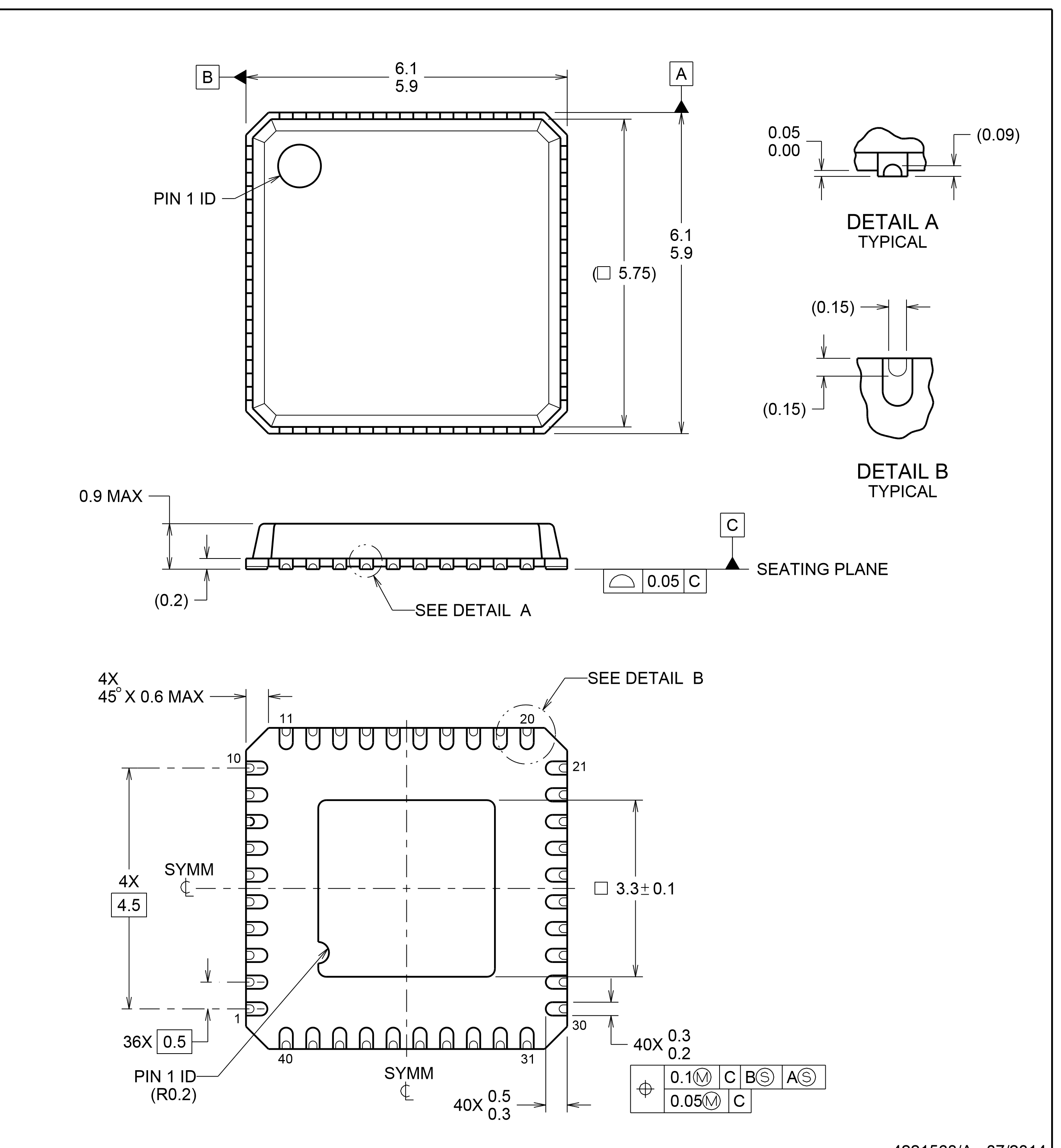
LM5140-Q1 is supplied in a 40-pin VQFN (RWG) measuring 6 mm x 6 mm with a 0.9 mm maximum height and a 0.5 mm pin pitch. The package has wettable flanks, which let an automated optical inspection station verify each solder fillet, a requirement on many automotive assembly lines. A large center exposed pad must be soldered to the board ground plane for both the thermal path and the analog/power ground reference. The orderable LM5140QRWGRQ1 ships in tape and reel. Package dimensions and the pin-1 orientation are shown below.
📄 Download the official TI LM5140-Q1 Datasheet (PDF)
Pin and Signal Definition
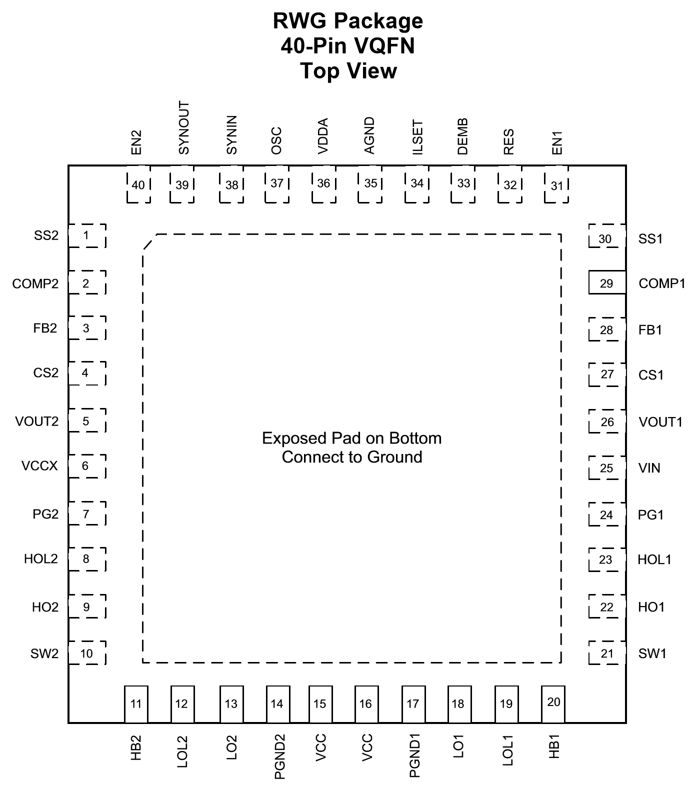
The 40 pins are organized as two mirrored channels (suffix 1 and 2) plus a shared bias and timing group. The key functional signals are:
- VIN: Power input, 3.8 V to 65 V, feeding the internal bias regulators and the high-side bootstrap path.
- EN1 / EN2: Independent per-channel enable inputs, allowing one rail to sequence or shut down without the other.
- FB1 / FB2: Feedback sense inputs; a resistor divider sets an adjustable output, or the pin is strapped for a fixed output.
- COMP1 / COMP2: Transconductance error-amplifier outputs for external loop compensation.
- CS1 / CS2: Current-sense inputs for the per-channel current limit and emulated peak-current control.
- HO1/HO2, HOL1/HOL2: High-side gate-driver turn-on and turn-off outputs; the split lets dead time and the rising edge be shaped independently.
- LO1/LO2, LOL1/LOL2: Low-side gate-driver turn-on and turn-off outputs.
- SW1 / SW2: Switch-node returns for the high-side drivers and bootstrap references.
- HB1 / HB2: High-side bootstrap bias supplies for the floating high-side drivers.
- VCC / VDD / VCCX / VDDA: Internal LDO output, driver bias, optional external bias bypass, and the quiet analog supply.
- PG1 / PG2: Open-drain power-good flags, one per channel.
- OSC, SYNIN, SYNOUT: Frequency-setting pin, external clock sync input, and clock output for cascading.
- ILSET, DEMB, RES, SS1/SS2: Current-limit set, diode-emulation select, restart/hiccup timing, and per-channel soft-start.
- AGND / PGND1 / PGND2: Analog ground reference and the two power-ground returns; the exposed pad bonds to both AGND and PGND on the PCB.
Alternative and Related Parts
The parts below are references within TI's wide-input controller family and the surrounding system. They are not drop-in replacements; verify channel count, input range, frequency and package before substituting.
| Part Number | Brand | Type / Key Difference | Package | Note |
|---|---|---|---|---|
| LM5140-Q1 (non-RWG options) | TI | Same die / alternate orderable / tape options | VQFN-40 | Same controller, ordering-code variants |
| LM5141-Q1 | TI | Single-channel wide-VIN buck controller | HTSSOP / VQFN | One channel where two are not needed |
| LM5145 | TI | Single 75 V synchronous buck controller | VQFN-24 | Higher-voltage single rail, industrial |
| LM25141-Q1 | TI | Single-channel 42 V wide-VIN controller | VQFN | Lower max VIN, single output |
| LM5160-Q1 | TI | Integrated-FET 65 V regulator (not controller) | HTSSOP | Choose when on-chip FETs at lower current fit |
Selection Tips: Choose LM5140-Q1 when a wide-input automotive board needs two independent, accurate rails with external FETs sized to the load and tunable gate drive for EMI. Step to LM5141-Q1 for a single channel, to LM5145 for a higher-voltage single industrial rail, or to an integrated-FET regulator such as LM5160-Q1 when the per-rail current is low enough that on-chip switches simplify the design.
Manufacturer Information
Texas Instruments Incorporated, headquartered in Dallas, Texas, USA, is one of the world's largest analog and embedded-processing semiconductor companies. The LM5140-Q1 belongs to TI's wide-VIN buck-controller portfolio, a line built around the SIMPLE SWITCHER and wide-input controller families that emphasize wide operating range, automotive qualification and robust protection.
For automotive power, TI pairs controllers like LM5140-Q1 with a deep catalog of compatible power MOSFETs, gate-drive support and reference designs, plus the AEC-Q100 qualification, functional-safety documentation and long-term supply that vehicle programs require. That ecosystem lets a designer move from a single-rail to a dual-rail wide-input supply, or scale current by choosing different external FETs, while staying inside one well-supported vendor family.
Applications



Frequently Asked Questions
Is LM5140-Q1 a complete regulator or a controller?
It is a controller. LM5140-Q1 provides the loop control, split gate drive and protection for two synchronous buck channels, but the power MOSFETs and inductors are external. That is what lets the same part serve very different output currents simply by changing the external FETs, rather than being capped by on-chip silicon.
What input voltage range does it support?
The operating input range is 3.8 V to 65 V with a 70 V absolute maximum, which covers an automotive 12 V battery line through cold-crank dips and load-dump transients without a separate pre-regulator.
Why does it have separate HO/HOL and LO/LOL pins?
The gate drivers split their turn-on and turn-off outputs so the designer can set the rising and falling edges, and therefore dead time, independently. Slowing turn-on with a resistor reduces EMI while a fast turn-off preserves efficiency, which helps automotive boards meet CISPR 25 limits.
Can the two channels run at different output voltages?
Yes. The two channels are independent: each has its own feedback, soft-start, enable and power-good, and each output is pin-selectable to a fixed value or set by a resistor divider anywhere from 1.5 V to 15 V. They share only the bias supply and the oscillator, and run 180 degrees interleaved to reduce input ripple.
Disclaimer
Information Accuracy: The specifications on this page are based on the official Texas Instruments LM5140-Q1 datasheet (SNVSA02A). We work to keep the information accurate and complete, but parameters can change with product revisions, so design engineers should verify all values against the latest official documentation before final design.
Product Authenticity Guarantee: All parts we supply are genuine factory originals with full material traceability.
Technical Support: Pre-sales and post-sales technical consultation is available free of charge.
Application Notice: This page is for reference only. Suitability for a specific application should be confirmed by the design engineer against the actual system requirements.
LM5140QRWGRQ1 Specifications
- Specifications
- Attributes
- Property Value
- Manufacturer
- Texas Instruments
- Series:
- -
- Package/Case:
- 40-VFQFN Exposed Pad
- Packaging:
- Tape & Reel (TR)
- Part Status:
- Active
- Output Type:
- Transistor Driver
- Function:
- Step-Down
- Topology:
- Buck
- Number of Outputs:
- 2
- Output Phases:
- 1
- Qualification:
- AEC-Q100
- Voltage - Supply (Vcc/Vdd):
- 3.8V ~ 65V
- Frequency - Switching:
- 440kHz, 2.2MHz
- Output Configuration:
- Positive
- Duty Cycle (Max):
- -
- Synchronous Rectifier:
- Yes
- Grade:
- Automotive
- Clock Sync:
- Yes
- Mounting Style:
- Surface Mount, Wettable Flank
- Operating Temperature:
- -40°C ~ 150°C (TJ)
- Serial Interfaces:
- -
- Control Features:
- Current Limit, Enable, Frequency Control, Soft Start
- Supplier Device Package:
- 40-VQFNP (6x6)
- Category:
- DC DC Switching Controllers
LM5140QRWGRQ1 Relevant information
- LM5140QRWGRQ1 Tags
- Popular Search
The following parts are popular search parts in DC DC Switching Controllers.
The Posts
-1,80mm.jpg)
-
GRM31CR61H106KA12L Murata MLCC: Applications, Selection and Buying Notes
GRM31CR61H106KA12L Murata MLCC guide for 10uF 50V X5R 1206 use, obsolete-status review, alternatives and sourcing checks.
-
GRM31CR61E476ME44L Murata MLCC: Applications, Selection and Buying Notes
GRM31CR61E476ME44L Murata MLCC guide for 47uF 25V X5R 1206 decoupling, alternatives and sourcing confirmation.
-2,70mm.jpg)
-
GRM32ER71H106KA12L Murata MLCC: Applications, Selection and Buying Notes
GRM32ER71H106KA12L Murata MLCC guide covering applications, selection, alternatives and sourcing checks for 10 uF, 50V, X7R, +/-10%, 1210 MLCC.
-0,55mm.jpg)
-
GRT155C81E105KE13D Murata MLCC: Applications, Selection and Buying Notes
GRT155C81E105KE13D Murata MLCC guide covering applications, selection, alternatives and sourcing checks for 1 uF, 25V, X6S, +/-10%, 0402 automotive MLCC.
-
GRM155C81E105KE11D Murata MLCC: Applications, Selection and Buying Notes
GRM155C81E105KE11D Murata MLCC guide covering applications, selection, alternatives and sourcing checks for 1 uF, 25V, X6S, +/-10%, 0402 MLCC.
-
GRM155C80J106ME11D Murata MLCC: Applications, Selection and Buying Notes
GRM155C80J106ME11D Murata MLCC guide covering applications, selection, alternatives and sourcing checks for 10 uF, 6.3V, X6S, +/-20%, 0402 MLCC.
-
GRM31CR61A476ME15L Murata MLCC: Applications, Selection and Buying Notes
GRM31CR61A476ME15L Murata MLCC guide covering 47uF 10V X5R 1206 use, derating, alternatives and procurement checks.
-
GRM31CR60J107ME39L Murata MLCC: Applications, Selection and Buying Notes
GRM31CR60J107ME39L Murata MLCC guide for 100uF 6.3V X5R 1206 rails, derating, alternatives and sourcing checks.
Related Products
-
LTC3728LEUH-1#TRPBF
Analog Devices Inc.
-
LT3782AIFE#TRPBF
Analog Devices Inc.
-
LTC1735IS#TRPBF
Analog Devices Inc.
-
LTC1735IS-1#TRPBF
Analog Devices Inc.
-
LTC3727EG#TRPBF
Analog Devices Inc.
-
UC3874DW-1
Texas Instruments
 PKG.jpg)
-
ISL78223AAZ
Renesas Electronics Corporation
-
UC2886D
Texas Instruments
-
UC3874N-2
Texas Instruments
-
UC3874DW-2
Unitrode
-
UC3874DW-2
Texas Instruments
-
UCC2806DTR
Texas Instruments


