Free Shipping Over$200

- Products
- Marking
- Alternative

How a Ferrite Bead Tames Supply Noise
How a Ferrite Bead Tames Supply Noise
A ferrite bead is not a little inductor placed wherever a rail looks noisy. It is a lossy high-frequency impedance inserted at a boundary, and it works only when that boundary, the return path and the nearby capacitors are chosen together.
On an AI or sensor board, the bead may sit between a switching regulator and an analog island, between a digital processor rail and a camera or RF section, or near a connector that brings noise onto a local supply. In each case the job is the same: let DC current pass, add loss where noise energy lives, and avoid making a new resonance that becomes harder to debug than the original ripple.
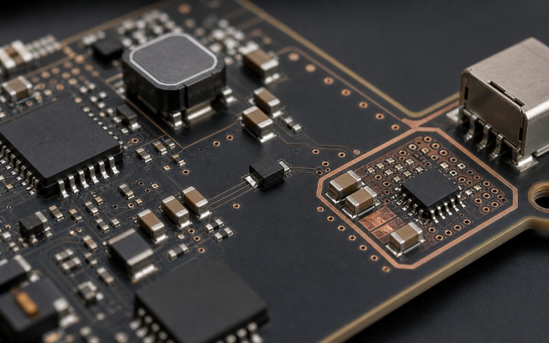
Treat the Bead as a Boundary Part
A bead belongs at a boundary. One side is the noisy source or the shared rail, and the other side is the circuit that needs a cleaner local supply. If the bead is placed in the middle of a long, shared trace, noise can couple around it through plane impedance, ground return, nearby signals and package capacitance.
The protected side needs local capacitance. Without capacitors after the bead, the quiet circuit has to pull fast current through the bead, which raises impedance exactly when the load asks for charge. With capacitors placed close to the load, the bead handles high-frequency isolation while the capacitors supply short current movement.
The source side also matters. A switching regulator with high ripple, a motor driver rail or a radio burst can excite the bead differently from a mild digital rail. The review should name the source of the noise instead of treating the bead as a universal part.
A good schematic marks the boundary clearly. A good layout makes it physical: short trace into the bead, short trace out of it, output capacitor pads close by, and a return path that does not force the quiet current to share the noisy loop.
Read the Impedance Curve, Not One Number
Ferrite beads are often marketed by impedance at a single frequency, such as an impedance value near a high-frequency test point. That number is a label, not a design answer. The full impedance curve shows where the part behaves more resistively, where it looks inductive, where package capacitance appears and how much loss it can add across the noise band.
The noise band should come from measurement or from a known switching frequency and harmonic range. A bead with a high headline impedance outside the board's noise range may do little. A lower impedance part with better loss at the noise energy band can perform better in the actual circuit.
The curve also tells where resonance can appear with the output capacitor. A bead and capacitor form a filter, and the filter can ring if the impedance, capacitance and source impedance create a sharp peak. Damping may come from capacitor ESR, bead loss, a small series resistor in some cases or a different value mix.
Do not compare beads only by the largest catalog impedance. Compare impedance across frequency, DC resistance, current rating, temperature rise, package size and the capacitor network around the bead. The right part is the one that damps the measured noise without starving the protected circuit.
Current Rating Changes the Impedance
A ferrite material can saturate under DC bias. As current rises, the effective impedance can fall, and the bead may lose much of the loss that made it attractive in the catalog. That is why the rail current and peak current must be part of the selection step.
The DC current rating should be checked with margin for operating temperature and burst behavior. A bead feeding an analog rail may carry modest current, while a bead feeding a camera module, RF stage or processor sub-rail can see pulses. The bead must keep enough impedance at the real current, not at a no-bias test condition.
DC resistance creates voltage drop and heat. A part that attenuates noise may still be wrong if it drops too much voltage during a load event or warms up near a heat source. The voltage budget and thermal location should be checked before a smaller package is approved.
Current direction is not the issue. The issue is magnetic bias, copper path and heat. If the bead is near a regulator inductor, shield can or hot processor, its temperature may rise before ripple loss is counted. That local environment should be part of the package decision.
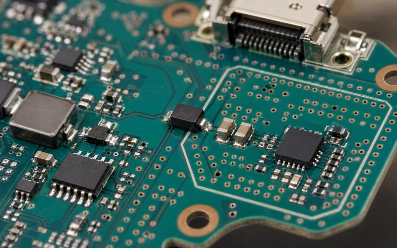
Place Capacitors on the Side That Needs Quiet Power
The output-side capacitor is not a decoration. It gives the quiet circuit a local charge source and sets the filter behavior with the bead. The first capacitor after the bead should be close to the protected load or local island, with a short return path to the same reference plane used by the load.
A common error is to put a bead in series with a rail, place a capacitor on the source side, and leave the protected side dependent on a long trace. That arrangement can reduce some conducted energy while leaving the local load exposed during a fast current edge.
Capacitor value and technology should match the noise and the load. Small MLCCs can work at high frequency, larger ceramics can support a broader band, and a small amount of ESR can help damping in some networks. A blind stack of low-ESR capacitors can create a sharp impedance peak.
The return path should be as deliberate as the series trace. If the quiet-side capacitor returns through a noisy ground slot or shares a narrow via with switching current, the bead cannot create a clean local island. Power and ground geometry decide whether the filter exists on the board or only in the schematic.
Check the Bead Against Regulator Stability
A bead placed after a regulator changes what the load looks like to the converter. Depending on feedback location and compensation, the converter may see less output capacitance, more phase shift or a different transient load. A regulator that is stable with direct capacitors may behave differently when a bead separates part of the load.
If the regulator senses before the bead, the quiet island can dip during a transient while the converter output looks acceptable at the feedback point. If the regulator senses after the bead, the bead can become part of the control path. Both arrangements need measurement at the protected load.
Startup can also change. A bead and quiet-side capacitor bank can slow local rail rise, interact with power sequencing or create a visible step when a downstream load turns on. That behavior should be checked with cold start, warm restart and the real enable order.
A bead should not be used to hide an unstable converter, poor loop layout or undersized decoupling. It is a filter boundary. If the source rail rings before the bead is added, the first fix may be regulator layout, compensation, input path, output capacitor choice or measurement method.
The regulator data sheet often gives allowed output capacitor ranges and stability notes. Treat those notes as part of the bead review. If the bead isolates part of the output bank, the converter may no longer see the capacitance the schematic appears to provide. The measurement plan should compare regulator output and protected-load voltage at the same time so the added filter does not move the problem from one node to another.
Use Layout to Keep Noise From Bypassing the Bead
Noise does not have to pass through the bead if the layout gives it an easier route. Plane slots, shared copper pours, adjacent high-speed traces, connector shields, enclosure metal and common ground impedance can all bypass a neat schematic filter.
The bead should sit on a visible narrow series path, with the protected island kept compact. The quiet-side capacitors should return to the quiet side of the island, then connect back to the main reference through a controlled plane path. The exact method depends on board stackup, frequency range and product safety rules, but the goal is to avoid a hidden shared loop.
Keep the bead away from high dV/dt switching nodes and high dI/dt current loops when placement allows. If the bead is routed next to the switch node or under a noisy inductor, it may pick up the noise it was meant to block. Physical distance, ground shielding and orientation can matter as much as the part number.
Board-edge rails deserve extra care. A connector-facing rail can bring cable noise inward or send local noise outward. The bead, ESD parts, input capacitor and connector ground should be placed so the current path faces the board edge in a realistic service direction and does not force the cable return through a sensitive island.
A layout review should trace both directions: how noise leaves the source and how current returns from the load. When the return path crosses the same gap the bead tries to create, the filter can be weakened. A clean bead placement is a physical loop-control decision, not a one-symbol schematic fix.
Set a Conservative Substitution Boundary
A ferrite bead substitute needs more than package size and impedance at one frequency. The boundary should include impedance curve, DC current rating, impedance under bias, DC resistance, temperature rise, material family, package size, voltage rating if stated, termination style and approved series.
A part with the same size and headline impedance can use a different ferrite material. That change can move the loss peak, reduce impedance at the rail current or change how the bead heats under ripple. A purchasing alternate should not be approved from a short parametric match alone.
The same rule applies to capacitor changes around the bead. Changing MLCC value, voltage rating, dielectric, package size or count can move the filter response. If a bead and capacitor network was measured as a pair, substitutes should be reviewed as a pair.
For production, keep a measurement record: source rail, protected rail, load profile, probe method, temperature, accepted bead series, accepted capacitor network and any placement limits. That evidence lets engineering approve later alternatives without repeating the same debate from memory.
When the product has EMI or noise margin problems, a bead change can move the result in either direction. Treat ferrite bead sourcing as an electrical approval item. A smaller DCR or larger impedance label does not automatically mean the board is safer.
Release Checklist for a Ferrite Bead
Before release, check the noise source, protected load, target frequency band, impedance curve, DC bias behavior, current rating, DC resistance, voltage drop, temperature rise, capacitor placement, damping, regulator stability, startup, load transient, return path, package height, assembly clearance and alternate list.
Then measure the board with the real load event. Compare the source side and quiet side of the bead, and use a probe setup that does not create its own loop. A clean result at one node is not enough if the protected circuit still sees the noise through ground, cable or nearby copper.
A ferrite bead tames supply noise when it is selected as a lossy boundary part and placed as part of a local power island. If the impedance curve, bias behavior, capacitors and layout path are reviewed together, the bead can reduce high-frequency energy without starving the circuit it protects.