Free Shipping Over$200

- Products
- Marking
- Alternative

Where Bulk Capacitance Buys Ride Through on a Load Step
Where Bulk Capacitance Buys Ride Through on a Load Step
Bulk capacitance buys time. It is the stored charge that keeps a rail from dropping too far while a regulator, an inductor and a control loop catch up with a sudden load. On an AI board that load can be a processor core, FPGA fabric, memory burst, radio event or camera pipeline waking at the same moment.
The mistake is to treat a bulk capacitor as a large value parked somewhere on the rail. A capacitor helps a load step only when its value, ESR, ESL, ripple rating, temperature behavior and placement match the time scale of the event. The wrong part can look generous in microfarads and still fail the board during a fast current edge.
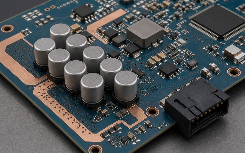
Start With the Load-Step Duration
A load step has both size and duration. A short burst asks the closest ceramic capacitors and plane pair to hold the first edge. A longer burst asks bulk capacitance to support the rail while the converter increases current. A long overload asks the regulator and thermal system to settle into a new operating point. Each time range needs a different part of the power network.
Estimate the charge needed during the gap between the load current increase and the converter response. The rough relationship is current times time divided by allowed voltage droop. That estimate gives a practical starting point, then ESR, ESL, bias, temperature and placement decide how much of the catalog value can be used.
The allowed droop should come from the load, not from a generic power rule. A processor core, DDR rail, camera sensor rail or RF power rail may have different limits during a transient. If the board has a cable, battery, hot-swap stage or long input trace ahead of the converter, the input side can also need bulk capacitance.
Measure the load step at the point that matters. A rail can look fine at the regulator output and sag at the processor pins because copper, vias and local decoupling add impedance. The capacitor bank should be evaluated against the load voltage, not a convenient test pad alone.
Capacitance Value Is Only the First Estimate
The printed capacitance value is a room-temperature starting number. Ceramic capacitors lose effective value under DC bias, small case sizes can lose a large share of their nominal capacitance, and some dielectric choices age over time. Polymer and electrolytic capacitors have different tolerance, leakage and lifetime behavior.
A large bulk value placed far from the load may help low-frequency movement while doing little for the first dip. A smaller value placed near the rail entry or load zone can be more useful during the time window the board cares about. Placement and impedance decide whether the capacitor bank participates in the event.
Use the converter data sheet and measured waveforms together. Some regulator control modes need a minimum or maximum output capacitance range for stability. Adding bulk capacitance without checking loop behavior can slow recovery, create ringing or shift the converter into a response the original design did not intend.
The load-step target should include effective capacitance after bias and tolerance. If the rail needs a minimum capacitance at voltage and temperature, the approved part list should state that boundary rather than listing only nominal values.
ESR and ESL Shape the First Dip
A load step usually creates an immediate voltage drop from ESR, then a slope from capacitance as charge leaves the capacitor bank. ESL adds another edge when current has to change quickly. The waveform shape tells which part of the network is limiting the rail.
Low ESR is not always the full answer. An ultra-low-ESR ceramic bank can create anti-resonance with larger capacitors and board inductance. A polymer capacitor may add useful damping while supplying more bulk charge. A mixed bank has to be checked as an impedance network, not as a sum of values.
The mounting path adds parasitics. Long traces, thin necks, shared vias and a distant ground return can make a low-ESR capacitor behave like a slower part. Wide copper, paired power and ground vias, short return paths and a clear plane connection allow the capacitor to work closer to its data-sheet behavior.
ESR also affects heating. Ripple current flowing through ESR creates loss inside the capacitor. A part that passes a capacitance calculation can run hot if ripple current or ambient temperature is high. Thermal rise should be checked at the same load profile used for the power rail.
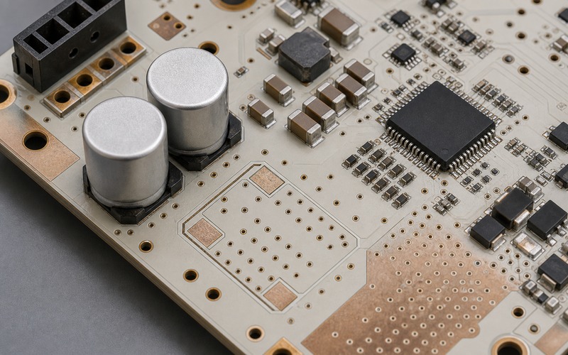
Choose the Mix by Time Scale
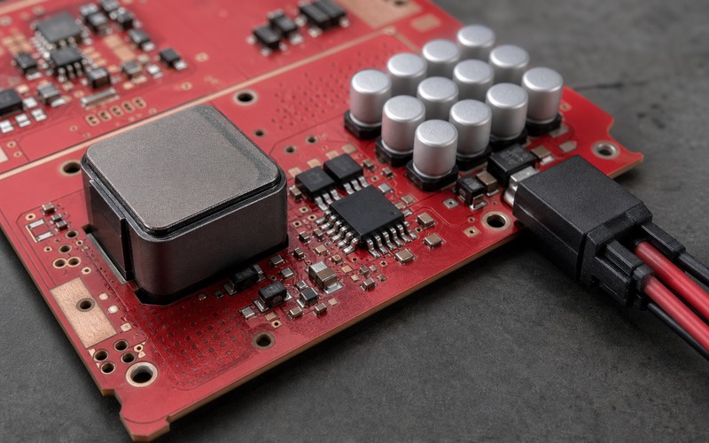
A robust rail often uses several capacitor types because no single package covers every time range. Small ceramics handle fast edges near the load. Mid-size ceramics and compact polymer capacitors cover intermediate movement. Larger polymer, tantalum polymer, aluminum electrolytic or hybrid parts may support longer steps near the converter or rail entry.
The mix should be intentional. Randomly scattering values can create impedance peaks, assembly cost and sourcing complexity without improving the rail. Start from the load-step profile, regulator stability range, target impedance and layout space, then choose the few values that solve a time-domain problem.
Check voltage rating with margin. A capacitor close to its rating can lose more capacitance, leak more current, age faster or have reduced reliability depending on technology. The allowed technology and voltage class should be part of the purchasing rule for each position.
Leakage matters for battery products and sleep states. A large capacitor bank can improve ride-through during an active burst while increasing standby current or startup time. The design should decide whether the stored energy helps the product more than it costs during off, sleep and wake transitions.
Placement Decides Whether the Charge Reaches the Load
Bulk capacitance should sit where charge can reach the current path without a narrow bottleneck. A capacitor near a connector may support input droop, while a capacitor near the converter output supports load-step recovery. A capacitor near the load can reduce local sag if the return path and plane connection are short enough.
The copper path between capacitor bank, regulator and load should be visible in layout review. If the route narrows around mounting holes, connector keepouts, heat-spreader screws or dense signal escapes, the bank may be weaker than the schematic suggests. The power path should be reviewed as geometry, not as a net name.
Via fields should connect the capacitor pads to the correct planes with short return paths. A bank of large capacitors on the top layer may still be isolated from the useful plane pair if the vias are too far away or share a crowded transition with high-current switching paths.
Mechanical access also matters. Large capacitors can interfere with heat sinks, shields, cables, enclosure ribs and automated inspection. A capacitor location that is electrically attractive but cannot be assembled or inspected consistently is not ready for production.
The input side and output side should not be confused. Input bulk capacitance helps the upstream source, cable, battery path or adapter ride through a sudden draw from the converter. Output bulk capacitance helps the load while the converter increases current. A board may need both, but each bank should be placed and measured against the job it serves.
Thermal copper can support large capacitor current paths, yet relief patterns and soldering needs can cut the path into small bridges. The release review should compare the electrical copper seen in layout with the manufactured pad and paste design. A capacitor with a strong catalog ripple rating can still underperform if the board gives it a weak path.
Read Ripple Current and Lifetime Together
Bulk capacitors often carry ripple current from the converter and from load movement. The RMS ripple rating is tied to frequency, ambient temperature, airflow and internal heating. Use the capacitor data sheet curves rather than a single headline number.
Lifetime is a thermal calculation for many bulk technologies. Aluminum electrolytic and hybrid capacitors age with temperature and ripple stress. Polymer capacitors have different aging behavior but still need ripple, temperature and voltage review. A product with a long service plan should keep these limits visible in the release record.
Surge, startup and hot-plug behavior belong in the review. A large bank can draw high inrush current, stress connectors, trip current limits or slow startup sequencing. If the converter starts into a discharged capacitor bank, the soft-start, current limit and upstream protection have to be checked together.
Acoustic and mechanical stress can appear in some designs. Board flex, vibration and thermal cycling can work on large capacitor solder joints. The layout should give enough pad support and spacing for the selected package technology and the product environment.
Give Purchasing a Controlled Alternate Boundary
A bulk capacitor alternate needs more than capacitance and voltage. The boundary should include technology, case size, height, capacitance tolerance, voltage rating, ESR range, ripple current rating, lifetime rating, temperature range, leakage, termination style, polarity if used and approved manufacturer series.
If a substitute changes ESR, the waveform can change. If it changes height, the enclosure or shield can fail. If it changes technology, leakage, lifetime and ripple behavior can move. The alternate rule should separate packaging changes from electrical substitutions that need engineering review.
Second-source testing should use the board's real load event. Compare voltage droop, recovery time, ringing, ripple heating, startup, inrush, light-load behavior and hot temperature operation. A capacitor that is fine on a bench supply may behave differently behind the actual converter and layout.
Keep the evidence with the board file. Record measurement point, probe method, load profile, ambient temperature, converter settings, accepted capacitor series and any placement limits. That record helps engineering and purchasing protect the ride-through behavior during future sourcing pressure.
The approved list should also state which changes are administrative and which changes are electrical. A reel quantity or packing suffix may stay in purchasing. A different capacitor technology, lower voltage rating, higher ESR band, shorter life rating, changed polarity style or taller case should return to engineering review before the part is used on production builds.
Final Bulk-Capacitance Checklist
Before release, check load-step amplitude, duration, allowed droop, effective capacitance after bias and tolerance, ESR, ESL, RMS ripple, temperature rise, lifetime, leakage, voltage rating, polarity, startup inrush, converter stability, input-side needs, output-side placement, copper width, via path, mechanical clearance and approved alternates.
Then verify the board with the final layout and real operating range. Use the same probe point and load profile for each candidate part. Each candidate part should be checked against the real electrical, thermal, mechanical and sourcing conditions it will face before the board moves into production.
Bulk capacitance is a time reserve, not a cure for every power problem. It buys ride-through only when the charge can move through the board at the moment the load asks for it. When value, ESR, placement, thermal life and substitute boundaries are reviewed together, the rail has a better chance of surviving the load step without becoming a late debug issue.