- Products
- Marking
- Alternative
iCE40UP5K for Ultra Low Power Edge Vision Preprocessing
iCE40UP5K for Ultra Low Power Edge Vision Preprocessing
iCE40UP5K belongs in the part of a vision product that wakes first and decides what deserves attention. It is a small FPGA, so it should not be treated as a full vision processor. Its value appears when a camera or image sensor needs a fixed, low power preprocessing stage before a host MCU, application processor or radio link wakes up.
The selection question is narrow: can the fabric capture enough of the pixel path, reduce the data, and hold a timing rule while the rest of the product stays asleep. If the answer is yes, the device can save host cycles and reduce bus traffic. If the algorithm needs a large frame buffer, heavy math or frequent model updates, another device class should carry that work.
Define the Preprocessing Job First
Preprocessing needs a concrete job description. It might crop a sensor window, watch line timing, count edges, pack bits, threshold pixels, merge a few simple features or wake a host when a pattern appears. Each job has a different cost in logic, memory blocks, clock rate and I/O pins.
A small FPGA is strongest when the operation is fixed and close to the input stream. A task that changes often, depends on a large software library or needs full-frame memory belongs outside this part. Keep the fabric job narrow enough that timing can close with room left for diagnostics and board variation.
The board record should name the input format, pixel clock range, control interface, output event and reset behavior. A phrase such as image preprocessing is too wide for purchasing or design review.
Keep the Camera Connector Honest
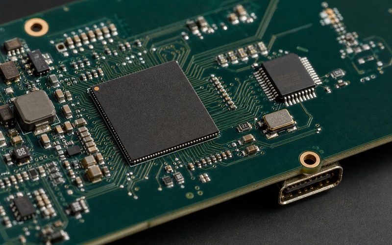
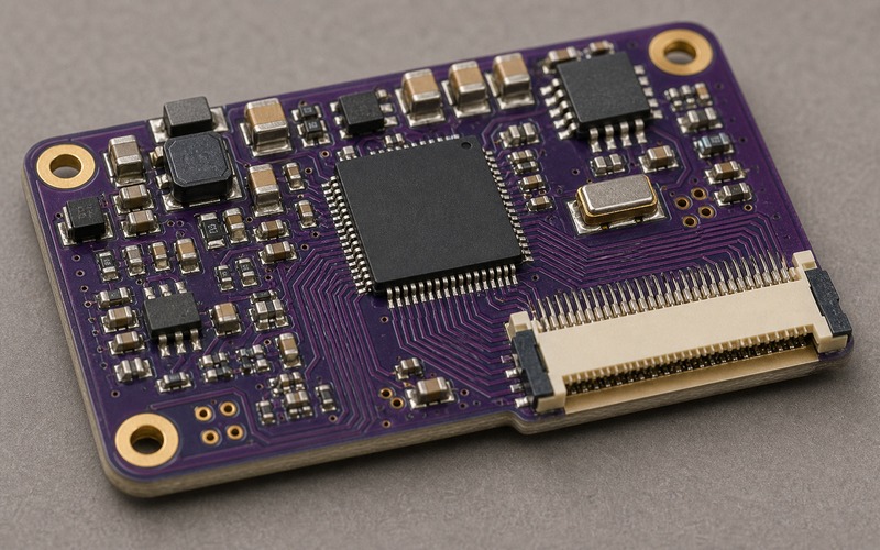
The camera or image sensor connector sets the board shape. It should sit at the board edge or along the cable path, with the opening facing outward. A flex cable that crosses the FPGA, oscillator or regulator area adds assembly risk and can change signal return paths. The local image assets use an edge-facing FPC connector for that reason.
Routing from the connector to the FPGA should keep short paths, a clear ground return and visible spacing. A tiny board can still suffer from a noisy clock, a weak sensor rail or a pin assignment that forces traces through a crowded corner. The picture of a clean module is useful only if the real board keeps the same discipline.
Check the sensor control lines with the same care as the pixel lines. Reset, standby, clock enable, I2C control and power enable pins often decide whether the module wakes cleanly from a low current state.
Power Is the Main Architecture Reason
iCE40UP5K is often considered because the host should sleep. That goal is lost if the support circuit burns current through a careless regulator, a weak pull-up network, a clock that never stops or a camera rail that stays on after the frame is ignored. The FPGA choice must be reviewed with the sensor, clock and power switch around it.
Measure the power path in states, not as one number. Record sensor off, FPGA configured, sensor clock running, line capture, event found, host wake and return to sleep. Each state should have a rail condition, clock condition and firmware condition. Without that state map, the board may look efficient in one bench test and fail the product battery target.
The low current design also needs a wake policy. Decide whether the FPGA wakes on every frame, a timed interval, a sensor strobe or an external event. That policy changes the regulator choice, oscillator choice and host interface.
Use Small Memory Deliberately
The device can help with line-level or window-level operations. It is not a place to hide a full image pipeline that needs large frame storage. Use small memory blocks for short buffers, line alignment, counters, flags and compact feature windows. If the job requires a full frame, the design should say where that frame lives and why this FPGA is still in the path.
Vision teams sometimes move too much into the first programmable device they can route. That creates a design that passes the first demo and becomes fragile when the sensor changes. A better use is to let the FPGA reduce traffic, clean timing, detect a small event or bridge a sensor format into something the host can read safely.
Keep a test pattern that proves the buffer behavior. A known pixel pattern should enter through the same connector and leave as the same event, counter or short packet that the product will use.
Clocking Decides Whether the Module Behaves
A vision preprocessing module can be small and still be clock-sensitive. The image sensor clock, FPGA internal clock, host interface clock and configuration clock may all meet near the same component. The design should name which clock owns each boundary and what happens during sleep and wake.
Clock startup matters. A slow oscillator, a rail that rises late or a sensor that starts output before the FPGA is ready can cause intermittent first-frame errors. That failure can look like model noise even though it comes from startup timing. Bring-up should include repeated wake cycles, not one continuous capture run.
Keep status bits for clock lock, frame start, line count, dropped pixels, buffer full and host wake. These bits cost little and help separate image content from board timing during field diagnosis.
Configuration and Update Boundaries
The configuration memory, programming access, reset path and boot mode should be checked before the package is approved. A tiny FPGA can be hard to recover if the programming pads disappear under a shield, camera bracket or enclosure feature. Leave a reachable service path for validation and manufacturing.
The update boundary needs a policy. If the FPGA image changes with the camera firmware, the product needs version matching and recovery behavior. If the bitstream is fixed for the product life, the approval record should state the sensor, clock, input format and feature stage that were used for that decision.
Configuration time also belongs in the state budget. A device that saves current after wake may still be wrong if it takes too long to become ready for the first useful frame.
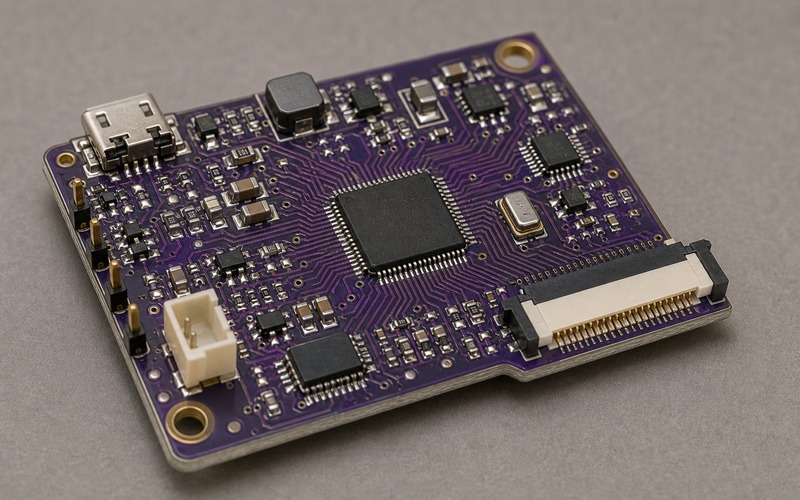
Package, Pins and Board Escape
Small packages bring real layout tradeoffs. Pin escape, FPC pitch, regulator placement, oscillator placement and test access need to fit on the same side of the board. A pin map that looks tidy in a spreadsheet can create a poor cable path or block a probe point.
Check I/O voltage with the image sensor and host. Level translation may erase the power gain if it sits awake all the time. Pull-up values, bank voltage and idle states should be recorded with the sensor mode that the product uses.
Thermal risk is low compared with larger processors, but heat still matters near image sensors. A warm regulator, radio or host processor can shift local temperature around the camera area. Keep the low power stage away from heat sources when the mechanical layout allows it.
Measure the Wake Chain as a Path
The wake chain starts before any image result exists. A timer, motion cue, sensor strobe, frame-valid signal or host request may turn on a rail, start a clock, release reset, load the FPGA image, enable the sensor and wait for a usable first line. Each event has delay and current. Put those events in order and measure them as a path, because a low current part can still miss the product target if wake time forces the host to stay awake longer than planned.
Use a repeated wake test rather than one long capture. Cycle the sensor rail, FPGA configuration, clock start and host wake many times while watching current, event flags and first-line validity. A fault that appears on the first frame after sleep may disappear during continuous streaming. That difference tells the team the problem is state transition, not vision quality.
Keep the output event small. A flag, counter, bounding window or short packet is easier to verify than a large image fragment. The host should receive a result that can be checked against a known test input during production and service. If the event format grows until it looks like a compressed frame, the design has probably moved beyond the job this FPGA should own.
Separate Image Noise from Logic Faults
Vision inputs are messy. Lighting, lens angle, sensor gain, motion blur and rolling shutter can change the pixel stream before the FPGA sees it. The preprocessing logic needs diagnostics that show whether an event was rejected because the image content changed or because the board dropped data. Line counters, frame counters, threshold counters, overflow flags and clock status bits give that separation.
Test with electrical patterns and optical patterns. An electrical pattern proves the FPC pins, I/O bank, clock and fabric path. An optical pattern proves the sensor, lens and lighting path. If both tests are mixed from the start, a wrong output can waste hours because no one knows whether the failure came from photons, pixels, routing or logic.
That separation also helps substitution work. A new sensor, oscillator, regulator or FPGA lot should run through the same electrical and optical checks. The team can then compare counts and timing against the approved board instead of relying on a visual impression of the camera image.
Substitution Review
An alternate small FPGA must match more than capacity. Check package, configuration mode, I/O voltage, memory blocks, oscillator support, tool support, programming path, current profile and lifecycle status. A replacement with similar logic can still break sensor timing or low current behavior.
The approved purchasing record should include the exact package, temperature grade, configuration memory, oscillator, regulator, sensor connector and allowed alternate conditions. If the design depends on a camera FPC orientation or a specific voltage bank, record that condition beside the part.
Supporting parts need their own alternates. A missing configuration flash, oscillator or low current regulator can block the module even when the FPGA is available.
Bring-Up and Production Checks
Bring-up should start with rails, configuration, oscillator, sensor reset and a simple input pattern. Only after those pass should the product feature stage be judged. This order prevents a board timing fault from being mistaken for vision behavior.
A production fixture does not need to run a full vision workload. It can check configuration, current in a few states, connector continuity, pixel clock presence, a short pattern and a host wake signal. Those checks prove the parts of the module that are hard to inspect later.
Keep the bitstream hash, test pattern, board revision and measured limits with the approval record.
Final iCE40UP5K Selection Checklist
Before approving iCE40UP5K, confirm the preprocessing task, sensor input, FPC direction, clock plan, configuration path, state current, I/O voltage, buffer size, debug status bits, test access and substitution boundary. Keep body links out of the article unless the target page has been verified as a working page.
The part is a strong choice when a tiny fixed vision stage lets the host sleep and the board proves its wake, capture and event path. If the design needs large memory, changing algorithms or full-frame processing, the work should move to a different device.