- Products
- Marking
- Alternative
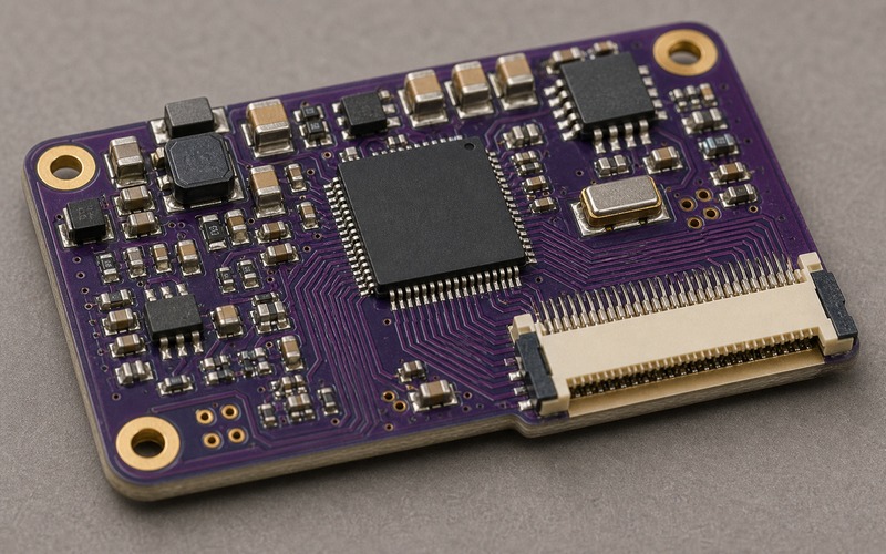
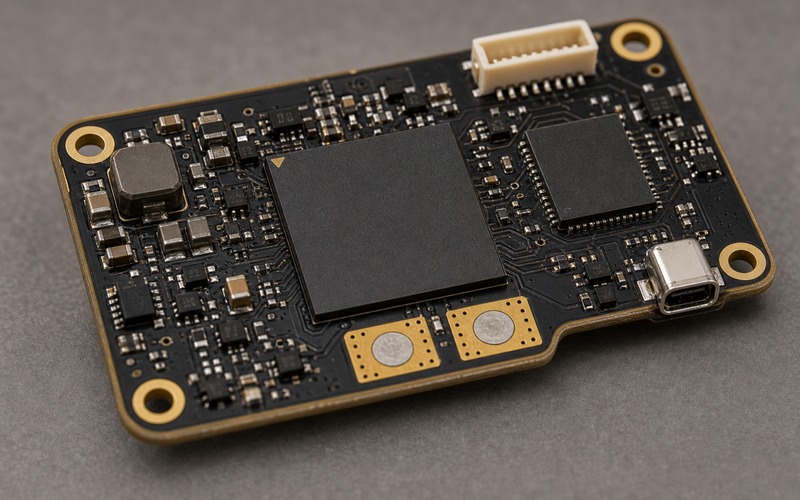
Alif Ensemble E7 Pairing an NPU with the MCU
Alif Ensemble E7 Pairing an NPU with the MCU
Alif Ensemble E7 belongs to a class of controllers that brings the neural engine closer to the real-time firmware. The idea is attractive when a product needs sensor handling, control logic and local inference inside one board-level decision. A separate application processor can be too large for the power budget, while a plain MCU can run out of compute headroom once feature extraction and classification are added.
The selection review should treat the device as a mixed workload part. The MCU side has to keep the product alive, safe and serviceable. The NPU side has to run the model within the available memory, timing and energy budget. The board has to support both sides with clean power, stable clocks, usable sensor inputs and a host path that does not become the hidden bottleneck.
Use an Integrated NPU When the Boundary Is Clear
An MCU with an integrated neural block is useful when the product has a bounded inference job. That job may be wake word filtering, vibration classification, sensor fusion, gesture recognition, low-rate audio features or a small vision preprocessing step. The workload should be narrow enough that model size, input rhythm and result latency can be measured on the target board.
The value comes from keeping real-time control near the inference result. A separate accelerator may need another interface, another rail, another boot path and another failure mode. A combined MCU plus NPU device can reduce that system cost when the model fits and the firmware can manage the shared resources cleanly.
The risk is treating the neural block as a magic reserve. It has a memory format, supported operators, bandwidth limit and toolchain path. If the model has to be reshaped heavily to fit, record the accuracy change and the reason. The board decision should follow measured evidence, not a benchmark headline.
Start with the Model and the Sensor Path Together
The model cannot be reviewed apart from the sensor. A motion model needs stable sampling and axis alignment. An audio model needs a known clock, clean microphone bias or digital microphone timing, and a defined feature window. A small vision path needs a sensor interface, frame timing and enough memory to hold the part of the image that matters.
Write the input path as a short engineering statement: sensor type, rail, interface, sample rate, window length, feature stage and result owner. If the statement cannot name the buffer, interrupt source and firmware task, the model is still a lab artifact rather than a product candidate.
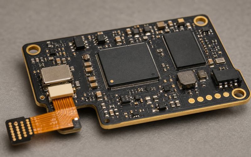
The sensor connector and routing need the same review as the processor. Lines that enter from the product edge should have protection, filtering or level translation when the environment requires it. A flex connector, camera connector, microphone path or inertial sensor bus should face the way the product will assemble and should not force the signal to loop around hot or noisy parts.
Plan Memory Before the Board Is Frozen
Memory planning decides whether an integrated NPU feels simple or painful. Count the firmware image, model weights, tensor arena, feature buffers, input history, communication buffers, logs, stack and any calibration data. A model that fits in a tool report can fail on a product build after diagnostics and update code are added.
External memory changes the board decision. It may solve capacity, but it adds routing, power, boot timing and supply risk. If the design depends on external flash, PSRAM or SDRAM, keep those devices in the selection record with their voltage, speed grade, package and layout assumptions. A substitute memory part can change timing enough to affect inference reliability.
Memory bandwidth also matters. An NPU can stall if data movement dominates the cycle. Keep the model, feature extraction and DMA paths visible during testing. If the firmware copies the same buffer several times, the measured latency may point to software architecture rather than neural compute.
Separate Always-On Tasks from Burst Inference
Many edge products spend long stretches in a low activity state. The MCU side may watch a sensor, maintain a timer, handle a bus or wait for a wake event. The NPU side may run only after a window is ready. That split should be reflected in the power plan and the firmware structure.
Measure the active profile as a sequence, not as one average current number. Capture sensor wake, feature extraction, NPU execution, result handling, communication and return to idle. The peak current can stress a small regulator, while a slow return to idle can dominate battery life. Both behaviors matter when the board has to run from a compact cell or a limited energy source.
Power domains need names. The core rail, I/O rail, memory rail, sensor rail and any camera or microphone rail should have startup order, current estimate, measurement access and fault behavior. If a rail is shared with a noisy load, the layout and decoupling plan should prove that inference and sensor readings remain stable.
Keep Firmware Ownership Visible
A combined MCU plus NPU device changes the firmware team boundary. One part may own sensor drivers, model conversion, inference scheduling, application state, communication and update behavior. That is efficient only when the responsibilities are written down and measurable.
Record which core or firmware task prepares features, which path starts inference, how errors are returned and what happens when the model times out. If the device has multiple execution domains, define the shared memory ownership and interrupt priority. Race conditions in the data path can look like poor model accuracy.
The toolchain belongs in the component decision. Model converter version, supported operator list, quantization method, firmware SDK, compiler version and debug path should be saved with the approval record. A future maintenance build should be able to reproduce the same result without guessing which tool state created the first working image.
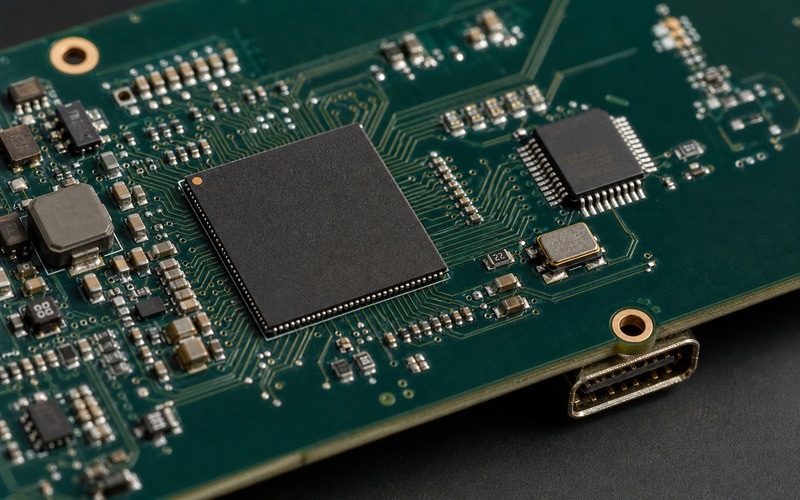
Review the Board Layout as a System
The processor package, memory and power devices should be placed as one timing and current system. Keep decoupling close, give high current loops a short return path, and avoid routing sensitive sensor lines through switching noise. A compact edge AI board can look clean while hiding a power or return-current problem under the package area.
Thermal behavior needs a practical check. An integrated neural block can create bursts of heat near the sensor, memory or regulator. The average temperature may be acceptable while a local hotspot shifts a nearby measurement. Use copper area, placement and duty cycle measurements to decide whether the heat path is safe for the product environment.
Connector orientation remains part of engineering quality. Host, camera, sensor, debug and board-to-board connectors should face the real cable or module path. A connector that points into the board center creates assembly stress and can teach the wrong design pattern when it appears in public technical material.
Make Bring-Up Evidence Easy to Repeat
The first board should prove more than a single successful inference run. Bring-up should record boot time, rail sequence, clock start, memory detection, sensor readiness, model load, inference latency, wake recovery and error reporting. Those measurements give the engineering team a way to compare firmware builds and board revisions without relying on memory.
Keep a small repeatable input set with the project. For motion work, include quiet, expected movement and vibration cases. For audio work, include different distances and background levels. For a compact vision path, include lighting and motion cases that stress the input stage. The goal is to see whether the board and model fail in a way the team can explain.
Debug access should remain useful after assembly. If the product covers the test pads with a shield, display, battery or enclosure wall, the team may lose the fastest route to diagnose a marginal unit. A production fixture also needs named signals, rail checks and a result path that can be repeated by someone outside the firmware team.
Define the Substitution Boundary
Substitution is harder for an MCU plus NPU device than for a simple controller. A replacement may match clock speed and package area but fail on model operator support, memory map, boot flow, power sequencing, debug access or peripheral timing. The substitute review has to include firmware behavior, model conversion and electrical ratings together.
A second option may be another neural MCU, a plain MCU plus an accelerator, an application processor or a small FPGA path. The right comparison depends on measured model size, latency, active energy, interface count, tool maturity and the amount of board change needed. Keep those measurements in the same place as the part number.
Purchasing should receive a clear boundary. The approved record should list package, temperature grade, rail requirements, memory pairing, clock source, toolchain, model format and accepted alternatives. If an alternate device requires model conversion or a layout change, it should not be treated as a pin-compatible purchasing swap.
Lifecycle review should also include the supporting parts. The memory device, regulator, crystal, connector and level shifter can block production as surely as the processor. Record which of those parts have approved alternates, which need firmware retest, and which require a new layout review. A neural MCU decision is a small system decision, so the supply plan should cover the system around the package.
If the buyer receives a request without those boundaries, price comparison can push the wrong part into the design. A lower cost package that changes temperature grade, memory timing or tool support may create engineering cost later. The approval note should make those tradeoffs visible before ordering begins.
Final Selection Checklist
Before approving an Alif Ensemble E7 style part, confirm the real sensor path, model size, memory budget, power sequence, wake behavior, host interface and firmware ownership. Check that the board has measurement access for the rails and signals with the highest failure risk. Confirm that every connector follows the real assembly direction and that no unverified link is needed to explain the design.
Also confirm that the same test image can be rebuilt, loaded and measured after a tool update. Reproducible build evidence keeps the hardware decision useful when the firmware team returns to the design months later.
Keep those files beside the measured board revision record.
The part earns its place when local inference reduces system complexity without hiding new risk. If the model fits, the power profile is measured, the firmware path is reproducible and substitution limits are clear, the integrated MCU plus NPU approach can be a strong product choice. If any of those points remain uncertain, the board should stay in validation until the evidence is complete.