- Products
- Marking
- Alternative
ATMEGA2560-16AU for Lightweight On-Device Sensing and Control
ATMEGA2560-16AU for Lightweight On-Device Sensing and Control
ATMEGA2560-16AU is often selected for products that need many ordinary control signals rather than a large inference engine. A small device may need to read switches, count pulses, sample slow sensors, drive indicators, switch relays, talk to a module and keep a predictable service port. In that kind of design, a stable 8-bit controller with a large pin count can be easier to approve than a faster part that brings extra software and layout risk.
The useful review starts with the real job on the board. The part has to match the number of inputs, the voltage domain, the timing rhythm, the package area and the firmware maintenance plan. A board that only needs bounded sensing and control can benefit from a controller whose behavior is easy to measure, whose peripherals are familiar and whose failure modes are visible during inspection.
Use the Part Where Predictability Matters
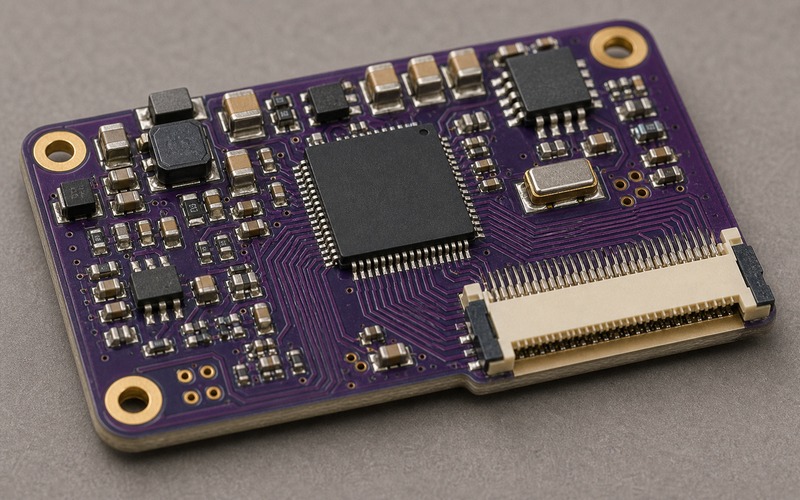
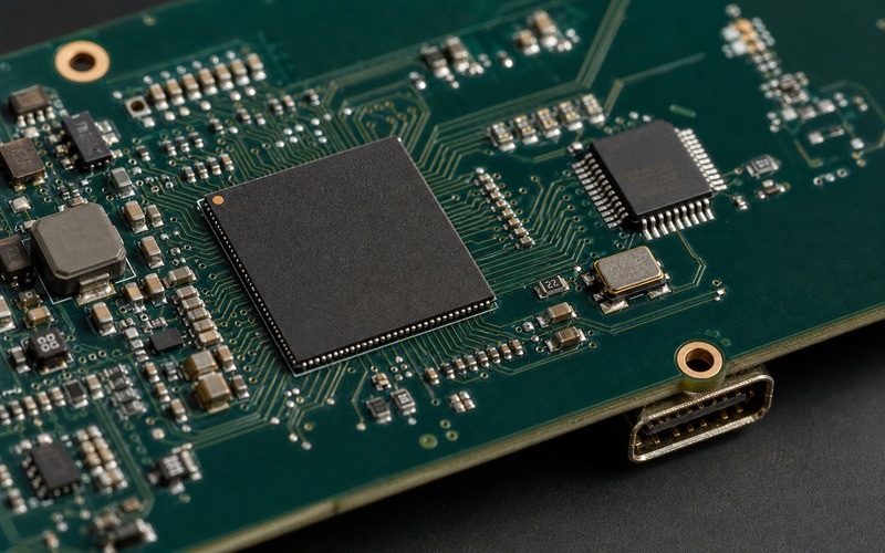
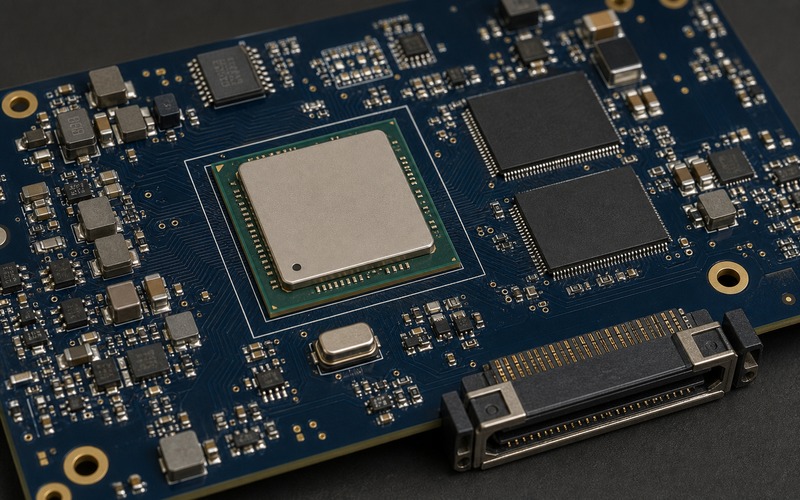
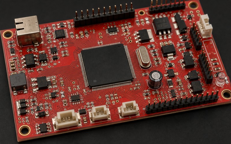
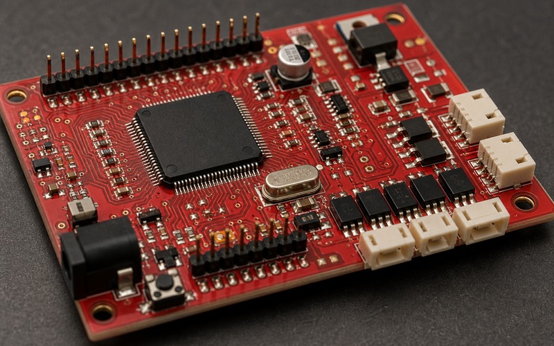
ATMEGA2560-16AU is the TQFP package version of a high pin count AVR microcontroller. It is not the right answer for camera inference, high bandwidth networking or heavy digital signal processing. It becomes useful when the product needs a clear map between pins, firmware tasks and board functions. That clarity helps engineering, purchasing and production review speak the same language.
Many small control boards spend their life reading slow inputs and changing outputs. They look simple until the exact number of lines is counted. A product may need several UARTs, extra timer channels, analog inputs, external interrupts, PWM outputs and a debug or service interface. A pin-rich controller reduces glue logic and can keep the board readable.
The selection note should state why an 8-bit controller is enough. If the sensor bandwidth is low, the control loop is slow, and the user interface is modest, a high clock 32-bit part may add little value. If the product needs secure updates, complex communication stacks or large local computation, the review should move to another controller class.
Start with Pin Count, Package and Voltage Domain
The suffix matters. ATMEGA2560-16AU points to a 16 MHz-capable device in a TQFP package. The package gives many pins in a board-friendly form, but it also demands routing space, inspection access and a soldering process that can hold fine leads without bridges. The board drawing should leave enough courtyard, test access and rework clearance.
Pin count should be reviewed from the schematic rather than from a memory of a development board. Count every sensor channel, control output, external interrupt, serial port, programming line, oscillator pin, reset circuit and spare line. A spare pin only counts if it reaches a useful place or a test point. Hidden spare pins inside a dense route rarely help during production recovery.
Voltage domain is the next decision. Many ATmega designs run at 5 V because legacy sensors, relays, opto inputs or industrial interfaces still expect that level. Other products use 3.3 V modules or radio parts. A mixed-voltage board needs level translation or careful part selection. Every connector should state what voltage a user or service technician can touch.
Check Sensor Inputs Before Firmware Assumptions
Lightweight sensing still needs a serious input path. A dry contact needs debounce and protection. A pulse sensor needs timer capture and an input edge that survives cable noise. An analog sensor needs reference planning, input filtering and enough settling time. A digital sensor needs bus pullups, address planning and a recovery method when the bus is held low.
The ADC path deserves special attention. ATMEGA2560 gives enough channels for many slow measurements, but the real accuracy depends on reference stability, source impedance, layout and firmware timing. A high impedance divider, long trace or noisy relay coil can move the reading. Use a defined reference strategy and leave a way to measure the analog rail.
Sampling rhythm should be written down. A temperature reading, a door switch, a flow pulse and a dimming output do not need the same timing. Group slow reads, reserve timer resources for signals that need them and avoid making a communication task block an input that sets a safety or fault state.
Plan the Communication Ports Early
Communication planning is a common reason to choose ATMEGA2560-16AU over a smaller controller. A control board may need one UART for a service header, another for a radio or display, SPI for a peripheral and I2C for slow sensors. Those ports should be assigned before the layout reaches the dense routing stage, because moving a serial port late can disturb a connector, timer or interrupt line.
Each port needs an electrical boundary. A short on-board UART is a different circuit from a connector that reaches a cable. SPI that stays near the MCU can be simple, while SPI that crosses a noisy board area may need stronger routing discipline. I2C pullups should match the rail and bus capacitance, and the firmware should have a recovery path if a slave holds the line.
Document the expected external partner for each interface. A display, radio, isolated link, service adapter or sensor module can bring its own voltage, wake timing and reset behavior. When those assumptions are visible, purchasing can review alternate modules without breaking the controller board.
Keep one practical rule in the approval file: every connector pin should have a named firmware owner, an idle state, a protection decision and a test method. That rule prevents unused-looking pins from becoming unclear field faults.
The same table also helps production build a fixture that checks real signals rather than cosmetic presence.
Review Control Outputs as Power Paths
A GPIO pin is rarely the whole output circuit. It may drive a transistor, a MOSFET gate, an optocoupler, a buzzer, an LED bank, a relay coil or a module enable line. The controller pin rating, driver threshold, pull state at reset and load behavior all belong in the component review.
Relay and motor loads need flyback paths, coil current checks and spacing that fits the product voltage. Indicator outputs need current limits and visibility targets. Module enable lines need a defined boot state so the board does not power a radio, sensor or actuator too early. A simple pin table can prevent a field fault that would be hard to diagnose after the housing is closed.
Thermal stress is usually handled by the driver parts rather than by the MCU, but the controller can still be damaged by poor output design. Long cables, inductive loads and user-accessible connectors need ESD, surge and reverse connection review. If the line leaves the board, treat it as an external interface rather than a harmless GPIO extension.
Keep Clock, Reset and Programming Paths Inspectable
The clock source sets the timing boundary. A ceramic resonator or crystal may be enough for local control, while serial links and time-sensitive pulse measurement may need tighter tolerance. Keep the load capacitors close, avoid routing noisy outputs under the oscillator area and record the oscillator choice with the firmware assumptions.
Reset behavior should be boring. Brownout settings, reset pullup, external reset access and supply ramp rate should all match the power tree. A board that starts cleanly on a lab supply can behave differently when a cable, battery, relay load or weak adapter is used. Test startup and recovery with the intended supply path.
Programming and service access belong on the product board. ISP pins, bootloader path, serial service connector or test pads should be reachable after assembly. If conformal coating, a display, a battery holder or a shield covers the access path, production will lose the easiest way to recover a failed unit.
Firmware Size, Peripherals and Test Evidence
The ATMEGA2560 family gives more program memory than smaller AVR controllers, which helps when a product has several peripheral drivers and a service interface. The firmware review should still count code size, SRAM use, interrupt load, stack margin and data logging needs. A controller can have enough flash and still fail because SRAM is fragmented or an interrupt path is too long.
Peripheral allocation should be stable before the layout is frozen. Timers, UARTs, SPI, I2C, PWM channels and external interrupts are shared resources. A late firmware request can force a board spin if every alternate pin has already been consumed. Keep a pin and peripheral table with the schematic review, and update it when the firmware changes.
Test evidence should match the real product. Record startup timing, ADC repeatability, pulse capture limits, worst-case output switching, communication recovery and watchdog behavior. The result is more useful when it includes board revision, supply voltage, load state and environmental notes. A clear test record makes later substitution and production support less dependent on memory.
Layout Checks for a Serviceable Control Board
A large TQFP controller can make the route look crowded. Keep decoupling close to the supply pins, separate noisy output current from analog returns and give the crystal a quiet area. Route sensor connectors toward the edge where the cable or harness enters the product. A connector that points into the middle of the board creates assembly stress and makes the article picture teach the wrong design habit.
Labeling in a real product can help assembly, but public article images should avoid readable text, fake markings and brand references. The technical value comes from the package, routing and surrounding parts. For the actual board, keep the test points and connector orientation clear enough for production inspection.
Mechanical clearance is part of the electrical choice. A 100-pin TQFP package may fit the schematic but fail the enclosure plan if the programmer, cable bend, heat source or fastening hole is ignored. Check the board area with the enclosure, service connector and cable path early.
Substitution and Purchasing Review
A substitute controller has to match more than memory size. Pinout, package, voltage range, oscillator options, timer allocation, bootloader method, programming connector, ADC behavior and reset settings all affect the board. A smaller AVR may save area but lose a UART or timer. A newer MCU may add performance but force level translation, new firmware tools or a different test fixture.
Before ordering or approving alternatives, keep the exact package suffix, clock requirement, voltage rail, programming method, firmware toolchain and allowed second-source strategy in the engineering record. If the product depends on 5 V tolerance or a specific pin map, that condition should be visible to the buyer and the engineer reviewing substitutes.
ATMEGA2560-16AU earns its place when the design values line count, predictable timing and maintainable firmware over raw compute performance. The final decision should be based on measured input behavior, output driver safety, power recovery, layout inspection and a substitution boundary that purchasing can follow without guessing. That boundary also keeps a later controller change separate from a board architecture change.