Free Shipping Over$200

- Products
- Marking
- Alternative

Filling a Wireless Link Out With RF Front End and Antenna Parts
A wireless link can fail while the baseband, protocol stack and power rails all look correct. The radio transmits, the packet format is valid, the firmware retries exactly as designed, yet the range is short, the sensitivity is unstable or certification margins collapse in a noisy chamber. That gap usually sits in the small parts between the transceiver pin and free space. The wireless IC may create the signal, but the front end, filter network, balun and antenna path decide what survives the trip out of the board and back into the receiver.
P3.28 is the point where a generic radio design turns into a link budget that can be deployed. It groups front end modules, filters, matching parts, chip antennas and GNSS gain blocks by the job they do in the path. Some parts add transmit power and receive gain. Some clean the band so unwanted energy does not flood the receiver or violate emissions masks. Some translate impedance and balance. Some turn board current into radiation, and some help a weak satellite signal make it through the first few centimeters of layout without being buried by downstream noise.
The RF path should be treated as a chain, not as a row of optional upgrades
A frequent planning mistake is to start with the radio SoC and treat the rest of the path as seasoning. Teams often assume they can place a transceiver, route a short trace to an antenna and then fix any shortfall with a stronger module later. Real boards rarely allow that. A front end module changes gain, noise figure, control timing, harmonic content, current draw and matching requirements. A filter inserts loss while improving selectivity. A chip antenna depends on ground clearance, board edge placement and keep-out volume. A GNSS low noise amplifier helps only if the preceding path has not already thrown the signal away.
The right design sequence begins with the link target. What range is needed, in what band, with what enclosure, battery budget and regulatory ceiling? How much conducted power can the radio source? How much loss appears in switch paths, feed traces, connectors, matching pads and the antenna itself? What blockers are nearby? Once those questions are written down, each RF part becomes a controlled decision instead of a rescue part added after the first range test disappoints the team.
QPF4288TR13 as a WiFi 6 front end module belongs in that early chain-level planning. A WiFi front end module can combine power amplifier, low noise amplifier and switching functions in a compact block, reducing discrete tuning work and giving the design a cleaner path to repeatable RF gain. It still has to be chosen against target band coverage, gain, bypass behavior, control logic, supply current, package thermal path and the radio that drives it. A front end module is useful when the radio alone cannot deliver the margin, but it is not a substitute for disciplined routing and antenna placement.
QPF4588TR13 as a WiFi 6E front end module pushes the same planning question into higher bands. Once the path moves into 6 GHz territory, layout tolerance, dielectric variation and loss stop behaving like small errors. The front end selection has to match the exact band plan, insertion loss budget and control scheme. A module that looks adjacent on paper may fail the actual design if its intended band split or matching environment does not line up with the transceiver and board stackup.
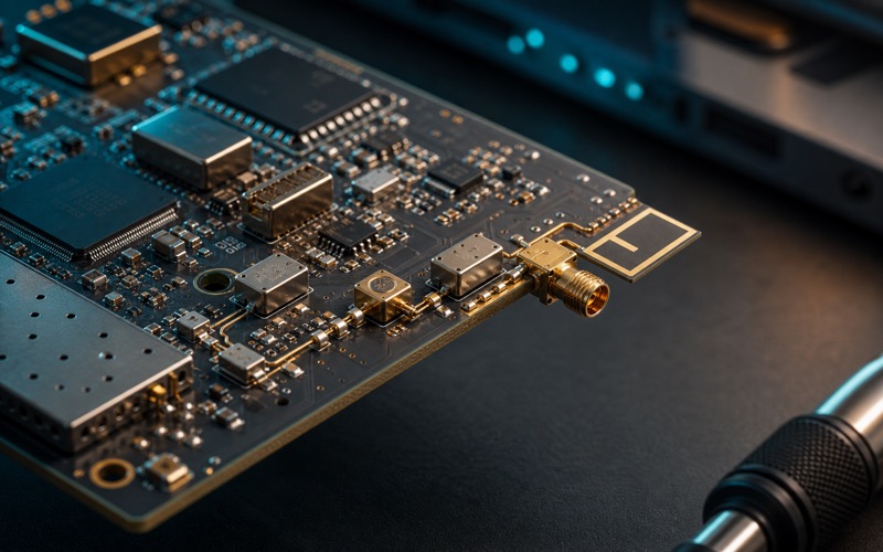
Front end modules add margin only when gain and linearity are both under control
SKY65981-11 as a radio front end module and SKY65971-11 as a radio front end module fit the wider discussion of integrated transmit and receive assistance. A front end module can improve transmit reach and receive sensitivity, but the real engineering question is how that gain behaves under coexistence, blockers and peak power conditions. If the upstream radio drives the module outside its intended operating range, or if the module sits next to a noisy DC DC converter and poor ground stitching, the board can gain conducted power while losing real packet reliability.
That is why linearity matters as much as headline gain. A short-range lab test may look better with more amplification, but a field deployment can be worse if the front end compresses under adjacent-channel energy or desensitizes the receiver during coexistence events. For battery devices, current draw has to be included in the same conversation. A stronger front end changes transmit burst current, supply decoupling needs and thermal rise. The system should ask whether the extra dB closes a deployment gap or whether the same range could be won by a better antenna position and lower feed loss.
The control interface also deserves more respect than it often gets. Many front end modules depend on clean timing between transmit, receive and bypass states. If the firmware or RF control GPIOs leave the module in the wrong mode during startup, the radio path can look dead or badly detuned. The part number is only the beginning. The module has to be wired into the system state machine with explicit sequencing, power-up defaults and validation in every band the product uses.
Filters and baluns decide whether the radio sees the band it thinks it sees
B39162B7504L210 as a SAW filter belongs where the receiver needs better band definition and out-of-band rejection. A SAW filter is not inserted because the schematic needs another RF rectangle. It is inserted because blockers, harmonics or emission limits demand selectivity. The cost is insertion loss, and that loss comes directly out of margin. The engineer has to decide whether the cleaner band justifies the reduction in signal level, and whether the filter is being placed at the point in the chain where it helps more than it hurts.
DEA205425BT-2028A4 as a 2.4 gigahertz balun represents another quiet but decisive function. A balun can convert a differential RF path to a single-ended antenna feed while also participating in impedance transformation. That means it affects both topology and match. A board that ignores the reference layout, keeps mismatched copper around the balun or treats its land pattern like an ordinary passive footprint can create a path that is technically connected and practically poor. The balun sits at a point where a few millimeters of careless layout can erase a long hour of protocol debugging.
Filtering and impedance translation should also be evaluated together. A SAW filter may expect a certain source and load environment. A balun may present a transformed impedance that changes how the following antenna network behaves. If each part is checked in isolation, the design can meet every single data-sheet fragment and still miss the system target. A wireless path is an interaction problem. Matching, filtering, grounding and enclosure influence one another.
The antenna path is a mechanical design disguised as an RF schematic
RFANT5220110A0T as a chip antenna is the clearest reminder that the radiating part of the path does not obey schematic optimism. A chip antenna is selected by band support, efficiency, size and matching range, but it lives or dies by where it sits on the board. It wants the board edge, clear keep-out volume, a reference ground shape the vendor has already characterized, and distance from metal, battery cans, displays, shields and high-speed noise sources. When teams tuck the antenna into whatever corner remains after mechanical packaging, they often create a link problem that no later front end upgrade can fully repair.
The feed line has to be treated like RF copper, not ordinary signal routing. Reference plane continuity, via transitions, nearby stitching, return current path and launch into the matching region all matter. The antenna network is also one of the first areas to drift when enclosure plastic, sealing gaskets, cables or a user's hand enter the picture. An antenna that looks acceptable on a bare board can move once the final product closes around it. The validation plan should include the assembled enclosure, likely installation position and nearby cables, not only the naked board on a bench.
Placement discipline is especially important on compact IoT boards where the wireless antenna competes with USB, display flex, battery leads and debug connectors for the same edge. The clean answer is usually subtraction. Move noisy circuits away, keep copper out of the keep-out, shorten the feed, and let the antenna have air. The product often gains more by protecting the antenna environment than by chasing another high-performance radio block.
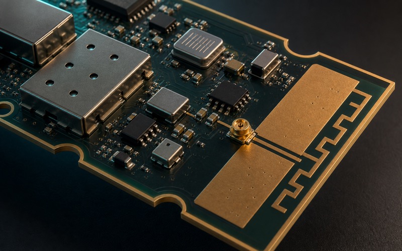
GNSS paths need quiet first-stage gain, not blind amplification everywhere
BGU8009 as a GNSS low noise amplifier represents a different problem from WiFi or general sub-GHz transmit links. A GNSS chain begins with signals that are already weak when they reach the antenna. The first gain stage matters because it shapes the system noise figure before later blocks get a vote. A low noise amplifier close to the antenna can preserve more of the useful satellite signal, but only if the preceding trace, bias network and power supply are quiet and the part is not being flooded by out-of-band energy.
This is where designers often confuse gain with improvement. If the antenna feed is long, the grounding is dirty or a nearby cellular or WiFi path is dumping energy into the same region, more gain can amplify the wrong problem. The GNSS LNA should be evaluated with filter strategy, bias stability, shielding and placement as one stack. It is helpful because it protects sensitivity early, not because every receiver becomes better when a random LNA is added.
A wireless BOM should be validated with substitution and coexistence in mind
P3.28 is also where supply-chain discipline enters RF design. A front end module replacement can change gain flatness, control polarity, harmonic behavior or matching assumptions. A different SAW filter can change insertion loss and rejection slope. Another balun can move the match enough to require re-tuning. A substitute chip antenna may fit the footprint while radiating differently inside the actual enclosure. RF substitution is rarely a pin-for-pin administrative change. It is a performance change that needs bench evidence.
The validation checklist should cover conducted measurements where possible, radiated checks in the real enclosure, current draw under transmit peaks, receive sensitivity with nearby blockers, GNSS performance with the main digital system active, and recovery behavior after the power path is stressed. The product should also be tested with the likely coexistence picture: Bluetooth next to WiFi, GNSS next to cellular, power converters switching nearby, USB or display traffic running, and the intended cable set attached. The quiet bench result is not enough if the deployment environment is noisy by design.
A strong wireless product does not treat the RF front end and antenna region as magic. It writes down the required margin, places the chain in the right order, chooses filters and baluns with the whole impedance environment in mind, gives the antenna real physical space, and protects the first receive stages from self-inflicted noise. Once that discipline is in place, the individual parts in P3.28 stop looking like optional accessories and start acting like the pieces that turn a radio block into a reliable deployed link.