Free Shipping Over$200

- Products
- Marking
- Alternative

K3LK3K30EM-BGCN as 8GB LPDDR5 Working Memory for Edge AI
K3LK3K30EM-BGCN as 8GB LPDDR5 Working Memory for Edge AI
K3LK3K30EM-BGCN is used as an 8GB Samsung LPDDR5 Package-on-Package memory device in compact application-processor platforms. In an edge-AI system, that memory holds the operating system, inference runtime, model weights, intermediate tensors, image buffers and application data while the processor is working. It is volatile working memory rather than boot flash or long-term storage. The distinction matters because adding storage capacity does not correct a shortage of inference memory, and adding DRAM does not provide retained data after power is removed.
The PoP construction also changes the mechanical and electrical task. The memory package is soldered directly above a compatible application processor instead of occupying an independent footprint beside it. This short connection can support a wide, fast LPDDR interface in a small board area, but the lower processor must provide the correct top-side land pattern, controller support, channel geometry and power behavior. A board cannot adopt this memory by drawing a generic LPDDR bus to an arbitrary SoC.
Public Samsung LPDDR5 family material provides useful architectural context, including family data rates up to 6,400 Mbps, an x64 bandwidth example of 51.2 GB/s, low-voltage operation and power reduction relative to LPDDR4X. Those are family-level figures, not guaranteed values for the BGCN suffix. The exact speed grade, geometry, ball assignment, voltage set, timing, package height and lifecycle status must come from controlled Samsung data or the original qualified platform records before design approval.
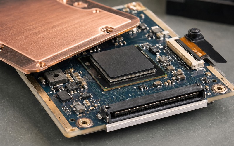
Confirm the exact memory role
An edge processor moves data through several memory domains. Nonvolatile flash stores the boot image, application and model files. On-chip SRAM serves small, latency-sensitive blocks. LPDDR5 supplies the larger working set used while the neural network and application are active. The capacity plan should separate these domains instead of treating every byte as interchangeable. Model compression may reduce flash size yet leave activation memory almost unchanged, while a higher-resolution input can increase temporary buffers without changing the model file.
Document which workloads must coexist: operating system, graphics, camera capture, pre-processing, inference, post-processing, network buffers and update services. Measure resident memory and peak allocation on the target software. The platform should retain margin for allocator fragmentation, driver reservations and later model revisions. An 8GB device can be generous for one vision pipeline and constrained for a multi-camera or multimodal workload, so the decision belongs to the complete use case rather than a headline capacity comparison.
Treat the full suffix as an engineering identity
The approved record must keep K3LK3K30EM-BGCN intact. A shortened description such as Samsung 8GB LPDDR5 loses the speed bin, organization, package and revision information encoded in the suffix. Closely related parts may share density and generation while differing in timing, voltage options, ball map, stack height or host qualification. The complete manufacturer number belongs in the bill of materials, processor compatibility record, assembly instructions, incoming inspection and software validation report.
The exact BGCN public product page is not available in Samsung's current public catalog, so parameters from another K3LK3K30EM suffix must not be copied into this design. A related suffix can indicate the device family, but it is not a substitute for the controlled specification. When maintaining a legacy board, use the original approved data, processor reference design, memory configuration tables and known-good build records. When starting a new board, obtain current manufacturer guidance before choosing this legacy identity.
Verify that the application processor supports this PoP
A PoP memory must match the processor mechanically and electrically. Confirm that the processor package exposes the required top-side PoP lands and that its memory controller supports the LPDDR5 generation, device density, channel count, data width, ranks and address geometry. Processor family names are insufficient because different package options can expose different memory interfaces. A controller may support LPDDR5 in a discrete layout yet lack a top-side pattern compatible with this memory package.
The processor vendor's qualified-memory list, reference schematic and layout rules should agree with the exact memory identity. Check whether the boot firmware already contains the necessary initialization parameters. If a platform was originally validated with BGCN, retain the matching processor package and configuration data. If either device changes, treat the combination as a new memory subsystem that needs signal, power, timing, thermal and software validation rather than a purchasing-only substitution.
Build a realistic 8GB capacity budget
Start with measured peak use, then add controlled margin. Model weights may be copied, mapped or transformed at load time. Activations depend on input shape, batch size, precision and accelerator scheduling. Camera and display paths reserve contiguous buffers that may be hidden from an application-level memory report. A Linux platform also uses memory for the kernel, page cache, graphics, network traffic and background services. Capture the high-water mark during long operation, model switching and error recovery.
A useful budget lists each major consumer and its worst simultaneous demand. Include double buffering where producer and consumer stages overlap. Account for secure regions, shared accelerator memory and firmware reservations that reduce the operating system's visible capacity. Leave room for field updates and diagnostic modes. If the measured margin is narrow, changing tensor precision, tiling the workload or reducing concurrent streams can be more practical than changing the PoP device after the board and processor package are fixed.
Translate data rate into application bandwidth
Samsung's current LPDDR5 family page describes products up to 6,400 Mbps and gives 51.2 GB/s as an x64 family example. That calculation is useful for understanding the architecture, but it does not establish the BGCN speed grade. Effective bandwidth is lower than the raw transfer figure because of command overhead, refresh, access patterns, controller arbitration, bank conflicts and power-state transitions. The neural accelerator, CPU, GPU, image processor and display controller may all compete for the same memory channels.
Create a traffic model from bytes moved per frame and frames per second. Include sensor input, color conversion, feature maps, model parameters, temporary tensors, display reads and storage or network copies. Then profile the target processor with representative software. Average bandwidth can look comfortable while short bursts stall a camera or accelerator. Record latency percentiles and channel utilization during the most demanding combined mode, especially when graphics and inference run together.
Keep memory access efficient for edge inference
Memory performance depends on software locality. Repeatedly moving large tensors between CPU, accelerator and graphics domains consumes bandwidth and energy even when arithmetic utilization is low. Use the processor vendor's supported zero-copy or shared-buffer mechanisms where they preserve coherency and security. Arrange tensor layouts for the accelerator, reuse working buffers and avoid format conversions that duplicate a full frame without a measurable benefit.
The 8GB capacity should enable a stable allocation strategy rather than encourage uncontrolled caching. Pre-allocate predictable pools for real-time paths, bound log and image caches, and test behavior when memory pressure occurs. A system that relies on swap storage during inference will add latency and flash wear. Long-duration tests should watch for fragmentation, leaks and growing caches because those faults may appear as a memory-component problem even though the physical LPDDR remains healthy.
Design all supply rails and sequences together
LPDDR5 uses multiple supply domains for the memory core, internal circuits and I/O. Samsung's family material lists low-voltage operating points such as a 1.05 V supply domain and 0.5 V I/O, but the exact rails, tolerances and sequence for K3LK3K30EM-BGCN must be taken from the controlled specification and processor platform guide. Do not infer the complete power tree from a family web page. The processor's memory I/O domain and the PoP device must share a compatible electrical plan.
Analyze cold start, warm reset, deep sleep, watchdog recovery, brownout and power removal. A valid steady voltage does not prove a valid ramp or shutdown. Prevent signals from back-powering an unpowered domain, and confirm the required discharge behavior before a restart. Place the specified decoupling close to the appropriate processor and memory supply lands. Measure droop and ringing at the stack during initialization, maximum traffic and low-power transitions, using a probing method that does not distort the result.
Preserve the LPDDR5 signal and reference structure
The PoP connection is short, but it still carries wide high-speed buses, clocks, command paths and reference-sensitive signals. Use the processor and memory design rules for impedance, escape geometry, layer transitions, reference planes and length relationships. The top-side processor substrate performs much of the interconnect, so the approved processor-memory pairing is essential. Board routing beneath the processor must still protect return paths and power integrity for the complete memory subsystem.
Review crosstalk, simultaneous switching noise and the effect of processor breakout vias on the power planes. Avoid routing noisy switching nodes beneath sensitive memory regions when the platform guide restricts them. Simulation should use the final package and board models where available. A copied reference layout remains valid only when package option, layer stack, materials, via construction and memory configuration match the reference assumptions.
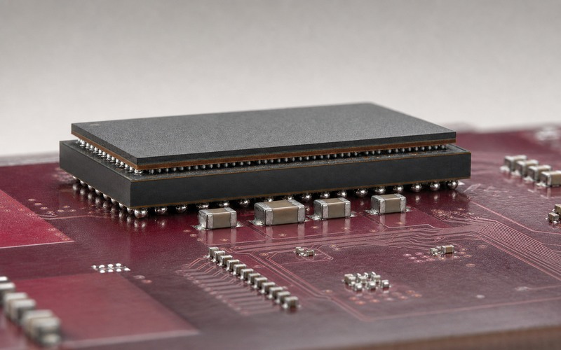
Initialize and train the exact geometry
LPDDR5 startup depends on correct mode-register values, timing tables, channel organization, frequency points and training behavior. These settings are often supplied by processor firmware rather than exposed in application code. The software team must know which memory identity and board revision each configuration supports. A system that boots at a low frequency can still fail when dynamic frequency scaling reaches a higher point or when temperature changes the timing margin.
Run training diagnostics on cold and hot units, across supply tolerance and after repeated resets. Exercise every supported operating frequency and low-power state. Preserve training logs and failure signatures from pilot builds. If the processor vendor provides a memory tool that generates parameters, store its version and input data with the release. An unexplained fallback to a slower rate should be treated as a validation failure, not accepted merely because the operating system starts.
Control the two PoP solder interfaces
PoP assembly creates one solder interface between the processor and PCB and another between the memory and processor. The upper and lower packages can warp differently during reflow, so paste, flux, temperature profile, placement force and component coplanarity matter. Use the exact Samsung and processor package drawings for land patterns, ball dimensions, package height, keep-outs and reflow limits. A generic BGA footprint cannot establish compatibility.
Agree with the assembler on PoP placement equipment, moisture handling, bake conditions, stencil strategy, reflow profiling and board support. The illustrated lifted heat spreader is an inspection view rather than an assembly method. Production should prevent mechanical load on the stack after reflow. Define X-ray views and acceptance limits for both joint levels; ordinary top inspection cannot reveal opens, head-in-pillow defects or bridges hidden within the stack.
Check stack height and enclosure clearance
The memory sits above the processor, making total stack height a direct enclosure and thermal constraint. Use worst-case package tolerances, solder collapse, board flatness, thermal-interface compression and enclosure tolerance. A heat spreader must contact the intended surface with controlled pressure. Excessive compression can bend the board or load hidden joints, while excessive clearance can leave the processor without an effective thermal path.
Keep screws, clips, battery cells and connector insertion forces from flexing the PoP area. If the product uses a thin board, model support during assembly and service. Drop, vibration and thermal cycling can reveal faults that a bench test misses. Record the approved mechanical stack with drawings and measured sample data so a later change in thermal pad thickness or enclosure tooling does not silently alter load on the memory assembly.
Manage heat from the processor beneath the memory
PoP saves board area but places the memory over a major heat source. The processor's inference load raises the temperature of both packages, and memory traffic adds its own dissipation. Review the temperature limit from the exact memory specification and measure near the stack under sustained combined workload. A short inference demonstration may stay cool while a sealed enclosure reaches equilibrium after an hour.
Build a thermal path that removes heat without concentrating force on the package. A compliant interface and flat spreader can work when compression is controlled. Verify throttling behavior, memory error rate and training margin at the hot condition. If the processor reduces frequency, confirm that camera and control deadlines remain valid. Thermal qualification should include low ambient start, high ambient operation and repeated transitions because package strain and electrical margin change together.
Test memory beyond a simple boot
A boot test covers a small portion of address space and timing behavior. Production and qualification tests should exercise data patterns, address transitions, channel loading and the supported frequency range. Run at voltage and temperature corners on representative units. Include long stress periods while the accelerator, camera and display generate realistic traffic. Capture corrected and uncorrected error indicators exposed by the processor platform.
Software tests should allocate and verify large regions, then repeat after suspend, resume, warm reset and frequency changes. Watch for failures correlated with a particular channel, temperature or workload transition. X-ray samples and board-level electrical results should be linked to lot and assembly data. That traceability helps separate component defects, reflow variation, processor-substrate problems and incorrect firmware settings.
Approach replacement as a platform requalification
A substitute cannot be approved from density and LPDDR5 generation alone. Compare full suffix, organization, channel and rank structure, package outline, top-side land pattern, ball assignment, voltage domains, speed bin, timing, temperature grade and lifecycle status. Confirm support in the processor firmware and qualified-memory list. Even a pin-compatible option may require new initialization data or have different power and thermal behavior.
When exact controlled information for BGCN is unavailable, pause the substitution decision rather than filling gaps with another suffix. For a legacy repair, retain known-good records and verify authenticity, labeling, package condition and lot traceability. For a new design, a current memory paired with a supported processor platform is usually a lower-risk path. Prototype the complete combination and repeat boot, training, stress, sleep, thermal and assembly checks before releasing the change.
Use a final LPDDR5 PoP review checklist
Before release, confirm the full K3LK3K30EM-BGCN identity, 8GB capacity requirement, exact Samsung specification, processor package compatibility, controller geometry, firmware parameters, supported frequency points and supply sequence. Review decoupling, power integrity, reference structures, PoP land patterns, reflow limits, total height, heat-spreader pressure and enclosure clearance. Keep family-level figures clearly separated from exact-suffix limits in the design record.
Qualification should cover cold and hot training, all frequency states, combined inference and graphics traffic, suspend and resume, brownout recovery, long memory stress, thermal equilibrium, X-ray inspection and mechanical reliability. Purchasing and engineering should approve any alternative together. A successful memory choice is the one that remains electrically stable, mechanically sound, thermally controlled and reproducible across production, rather than one that matches only the words 8GB LPDDR5.