Free Shipping Over$200

- Products
- Marking
- Alternative

THGAF8G8T23BAIL as 32GB UFS 2.1 Storage for an Edge Device
THGAF8G8T23BAIL as 32GB UFS 2.1 Storage for an Edge Device
THGAF8G8T23BAIL is a KIOXIA 32GB Universal Flash Storage device, not an eMMC. The manufacturer's UFS product brief identifies it as UFS 2.1 with a published maximum data-rate figure of 1,160 MB/s, a 2.7 to 3.6 V main supply, a 1.70 to 1.95 V UFS interface supply, a -25 to +85 degree C operating range and an 11.5 by 13.0 by 0.8 mm BGA package. The speed figure is a manufacturer test result rather than a guaranteed application throughput number.
That classification changes the whole board design. UFS uses a low-pin-count serial link based on M-PHY and UniPro, supports full-duplex communication and expects a host controller, firmware stack and power sequence built for UFS. An eMMC controller and its parallel clock, command and data bus cannot operate this device. The part combines NAND flash with a controller that handles error correction, wear leveling, logical-to-physical mapping and bad-block management, but system-level data integrity still depends on the workload, power behavior, thermal profile and software.
Lifecycle status also belongs in the engineering decision. KIOXIA's April 2025 discontinuation notice lists THGAF8G8T23BAIL among the 32GB UFS 2.1 products reaching end of life, with the last-time-buy milestone in December 2025 and the last-time-shipment milestone in June 2026. A legacy board may still require the exact part, while a new platform should evaluate a supported UFS generation and validate the resulting package, voltage, software and capacity changes. The review below separates exact-part maintenance from a new design choice.
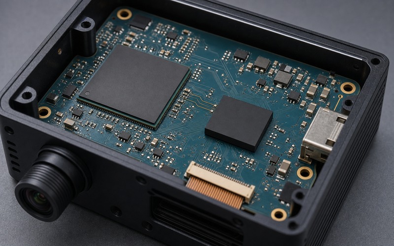
Correct the interface before making any schematic decision
The first gate is the SoC data sheet. Confirm that the selected processor exposes a UFS host controller that supports UFS 2.1 operation and the required M-PHY gear and lane count. A processor with SD, SDIO, eMMC or generic high-speed serial peripherals is not automatically suitable. The UFS host also needs a compatible reference clock strategy, reset or device-control method, link-startup firmware and boot-ROM behavior if the product must start from UFS.
Record the controller instance, pin multiplexing, supported gears, lane configuration and boot limitations in the schematic review. Some processors support UFS only on selected packages or only with specific I/O rails. Others can use UFS after the first-stage loader but cannot boot directly from it. Those differences affect the recovery medium, factory programming path and the amount of nonvolatile storage required elsewhere on the board.
Use the complete part identity
THGAF8G8T23BAIL identifies a specific 32GB UFS 2.1 product and package. Do not shorten the approved material record to a generic 32GB UFS description. The full manufacturer number belongs in the bill of materials, schematic attributes, footprint record, incoming inspection and software qualification report. Managed-flash products with the same nominal capacity may expose different descriptors, firmware behavior, power states and lifetime characteristics.
The internal product record should be treated as a part-number anchor, while electrical approval remains tied to the manufacturer specification and the actual host platform. Label punctuation, package height and lifecycle status need independent checks. A sourcing proposal that says only 'UFS 32GB' leaves the design team unable to determine whether the tested software, board escape and power sequence still apply.
Budget usable capacity instead of the printed density
KIOXIA states that the product density is based on the flash capacity inside the package and that user-available capacity is lower because of formatting, management areas, bad blocks and host or application constraints. Partition planning must therefore start from the capacity reported by the production device after the approved configuration, not from 32GB multiplied into a theoretical file count. Reserve space for boot images, recovery, update staging, logs and future file-system growth.
Edge products often write far more than their final stored data suggests. Camera clips, event indexes, model updates, databases and diagnostic logs create metadata and temporary writes. Measure daily writes and peak bursts on representative software. Keep a free-space margin so garbage collection and file-system maintenance do not run at the limit. A capacity plan should include the service interval and data-retention policy rather than relying on a single laboratory image.
Treat 1,160 MB/s as a ceiling from a defined test
The manufacturer's product brief publishes 1,160 MB/s as the maximum data-rate figure for this UFS 2.1 device. It also states that read and write speeds are best values from a specific test environment and are not warranted for every device. Application throughput depends on link gear, lane configuration, block size, read or write mix, file system, host controller, thermal state and the amount of internal maintenance underway.
Build a bandwidth budget from the real traffic. A vision device may read model assets while writing encoded video and rotating logs. The full-duplex link helps, but the host, DMA fabric and file system can still become the limiting stage. Measure sustained operation after the device has been filled and exercised instead of relying on a fresh sequential benchmark. Capture latency percentiles because a short storage pause can matter more than average throughput to a real-time pipeline.
Design the two supply domains as one sequence
The listed configuration uses a 2.7 to 3.6 V VCC rail and a 1.70 to 1.95 V VCCQ2 interface rail; the KIOXIA brief identifies it as dual-supply operation in which VCCQ need not be supplied. Verify the exact product specification before freezing the schematic. Both regulators must meet ramp, tolerance, noise and discharge requirements at the device pins, and the SoC I/O domain must be compatible with the interface rail.
A valid steady voltage does not prove a valid startup or shutdown. Analyze every case: cold power-on, warm reset, processor reset while storage remains powered, brief input interruption, watchdog recovery and deep sleep. Prevent signal-driven back-powering when one rail is absent. Firmware should not begin link startup until supplies and clocks satisfy the required conditions, and it should not cut power while writes or internal maintenance may still be active.
Give each rail local high-frequency support
Place the ceramic capacitors required by the product design guide close to their respective BGA supply balls, with short paths to ground vias. Keep the VCC and VCCQ2 regions identifiable in the layout so a late edit cannot attach a capacitor to the wrong plane. Use a continuous ground reference and avoid narrow shared necks that add inductance. The host-side interface rail deserves the same attention as the flash main rail.
Measure voltage at the package side of the decoupling network during link startup, sustained writes, sleep entry and wake. Use a short probe ground and enough bandwidth to see fast droop or ringing. Check regulator stability with the installed capacitor values and bias. Current consumption changes with transfer mode and background activity, so characterize representative workloads and thermal conditions rather than sizing from a single average number.
Route M-PHY lanes as controlled differential channels
UFS replaces the wide eMMC bus with high-speed serial transmit and receive lanes. Route each differential pair with the impedance, spacing, reference-plane continuity and loss budget required by the SoC and UFS design guides. Keep the pairs short, direct and isolated from switching regulators, high-current loops, clocks and noisy flex connectors. Avoid plane splits, unnecessary vias and test stubs in the active channel.
Pair matching cannot repair a poor return path. Maintain the same reference structure through the BGA escape, layer transitions and processor fan-out. When vias are needed, use a symmetric transition and provide nearby return vias. Review crosstalk and insertion loss on the final stackup. If the host supports two lanes, the lane mapping and polarity options must be documented rather than assumed from a reference board with a different package.
Handle reference clock, reset and sideband behavior explicitly
The storage link includes more than the data lanes. Confirm the host's reference-clock mode, frequency, jitter budget and low-power behavior against the product specification and the processor integration guide. Keep the clock away from noisy power nodes and protect its return path. Any reset, device-control or sideband signals need defined pull states while the host is held in reset or unpowered.
Firmware and hardware teams should agree on who owns link recovery. A timeout during startup may come from rail order, clock absence, signal integrity, unsupported gear negotiation or a device that never left a previous power state. Provide accessible measurement points on low-speed control signals without creating stubs on the high-speed lanes. Store the selected host-controller parameters with the board revision and test image.
Create the BGA footprint from the exact package drawing
KIOXIA lists an 11.5 by 13.0 by 0.8 mm BGA for THGAF8G8T23BAIL. The footprint still requires the exact ball map, pitch, ball diameter, keep-outs and package tolerances from the applicable drawing. A similar 11.5 by 13 mm managed-flash package may use a different ball assignment. The schematic symbol, footprint and escape pattern must be checked together and kept under revision control.
Review solder-mask definition, pad finish, via-in-pad process, filled-via requirements, paste strategy and X-ray inspection with the assembler. The low body height makes board warp and package coplanarity relevant. Define a pin-one check and an X-ray acceptance sample for the first build. Hidden joints mean a visual perimeter inspection cannot confirm opens, bridges or insufficient collapse beneath the device.
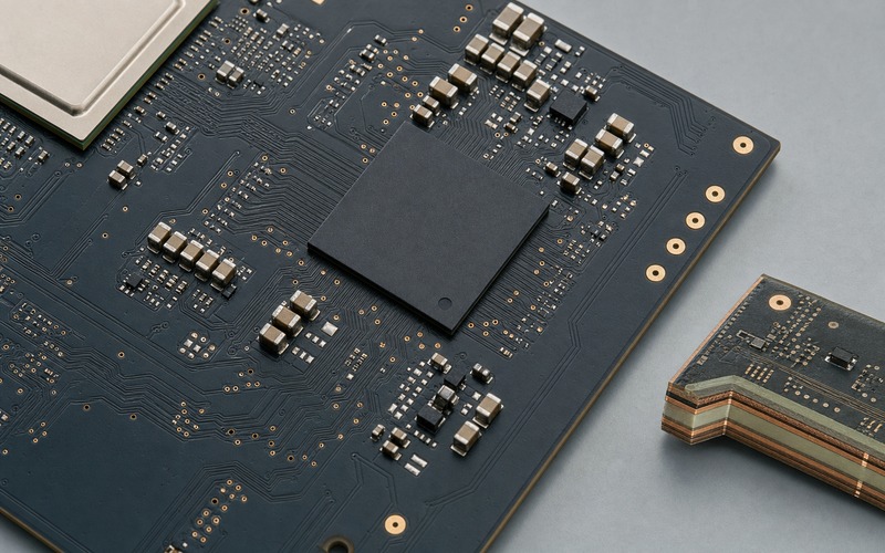
Keep the BGA escape away from mechanical risk
Place the UFS package close to the SoC but not beside board edges, screw bosses, large cutouts or connectors that bend the PCB during insertion. Avoid routing critical pairs through regions that see enclosure pressure or repeated cable force. If the board is thin, model deflection and establish assembly support. A storage device can pass electrical test and later develop intermittent BGA faults if mechanical strain is ignored.
Thermal expansion also loads BGA joints. Keep large heat sources and strong temperature gradients in the reliability review. Do not place a tall heat sink clamp across the storage package unless the mechanical stack is designed for it. Inspect representative units after thermal cycling and vibration when the product environment demands it. Board-level reliability belongs in the same approval as link performance.
Understand what the internal controller does
The managed-flash controller handles error correction, wear leveling, address translation and bad-block management inside the BGA. That removes raw-NAND management from the host, but it does not make every write equally harmless. The host still determines access patterns, free-space pressure, cache flushing, partitioning and power-loss exposure. Internal behavior can change latency as the medium ages or reorganizes data.
Do not build a health model from one benchmark. Record bytes written by the application, write amplification at the file-system level where measurable, temperature and power cycles. Use standard device health information supported by the host stack, and confirm how the platform exposes errors. A rising latency tail or repeated recovery event deserves investigation even if ordinary reads still succeed.
Protect data through sudden power loss
A managed device may acknowledge data at one layer while metadata or internal mapping work is still vulnerable to an abrupt rail collapse. Design the software so critical records use an atomic update method, checksums and recoverable metadata. Flush at defined transaction boundaries and verify what the operating system and UFS driver actually guarantee. Repeatedly cutting power during random writes is a required system test, not an exceptional demonstration.
Hardware should provide enough warning or hold-up time for the actions the design claims it can complete. If no controlled shutdown is possible, software must assume interruption at any instruction and recover from the previous valid state. Separate replaceable logs from essential configuration and keep a known-good boot or recovery path. A watchdog reset and a full power removal are different fault cases and should be tested separately.
Plan boot, recovery and factory programming
If the SoC boots from UFS, confirm that its immutable boot ROM supports the device generation, lane arrangement, boot logical units and security configuration. Define how an empty device is first programmed and how a failed field update returns to a bootable image. If the SoC cannot boot from this UFS part, retain a separate boot medium and make the handoff to UFS explicit in the startup design.
Factory programming must identify the exact device, apply the approved configuration, write images, verify every partition and record traceability. Avoid irreversible configuration changes before the image and power path are proven. A service fixture should recover a board whose application partitions are corrupt. Test recovery after interrupted programming, because that is when boot assumptions and access permissions are most likely to fail.
Review security features as a system
UFS can support protected storage functions, but their value depends on correct host authentication, key handling, life-cycle state and software policy. Decide which data needs confidentiality, integrity or rollback protection. Keep device-bound keys out of ordinary files and verify the processor's secure-boot and trusted-execution path before relying on a protected region for credentials.
Security configuration should be repeatable in production and auditable without exposing secrets. Define ownership of provisioning records, failure handling and service replacement. A replacement storage device may require new credentials or re-enrollment. Do not assume that a larger or newer UFS part preserves every protected-region behavior; verify the host stack and production tools with the exact candidate.
Validate temperature and sustained workloads
The listed operating range is -25 to +85 degrees C, but the relevant value is the package temperature inside the finished enclosure. Measure it while the processor, camera, radio and storage are active together. NAND retention, write behavior and controller throttling can all depend on temperature. A room-temperature copy test does not represent a sealed edge camera in sunlight or a fanless industrial node.
Run cold startup, hot startup, sustained mixed traffic, sleep and wake, and long idle retention on representative hardware. Fill the device to the expected service level before the stress run. Capture host errors, link recovery, throughput distribution and rail behavior. Thermal approval should include neighboring components and airflow because the storage package may be heated mainly by the processor rather than by its own average power.
Treat the lifecycle notice as a redesign trigger
KIOXIA's April 2025 notice identifies THGAF8G8T23BAIL as a discontinued 32GB UFS 2.1 product. It names THGJFPT0E18BAIP, a 128GB UFS 3.1 product in an 11.0 by 13.0 by 0.8 mm package, as the recommended product option. That is a migration direction, not a footprint-level substitution: capacity, UFS generation, package width, supply arrangement, host support and software behavior all need a fresh review.
For a legacy build, control the exact approved number and preserve test evidence. For a redesign, start with the SoC's supported UFS generations and current manufacturer options, then requalify power, signal integrity, footprint, boot, security, performance and endurance. Do not let a procurement substitution silently turn into a storage-architecture change. The engineering change record should show which risks were retested.
Use the verified product record as the part-number anchor
The verified THGAF8G8T23BAIL product detail page provides the exact model reference used by purchasing and engineering. The same path has been checked on both public domains. It does not replace KIOXIA's specification, UFS integration guidance or lifecycle notice, but it prevents the visible model link from pointing to a generic family or an unrelated package.
Keep the link text, bill of materials and incoming label aligned to the full part number. Attach the host-controller version, board revision, storage firmware identification and qualification report to the approval record. If a future candidate uses a different model, create a separate record and separate validation result instead of overwriting the evidence for this legacy device.
Final storage-subsystem checklist
Confirm that the device is 32GB UFS 2.1 rather than eMMC; the SoC has a compatible UFS host; boot and recovery are supported; VCC and VCCQ2 are sequenced correctly; differential lanes, reference clock and BGA escape follow the final stackup; and package, temperature and lifecycle facts match the complete part number. Verify usable capacity, sustained mixed traffic, sudden power loss, sleep, wake and factory programming.
For ongoing production, retain traceability and a realistic lifetime model. For a redesign, treat the named UFS 3.1 option as a new component and rerun electrical, mechanical, software, security and endurance approval. That discipline keeps a managed-flash convenience from hiding the interfaces and failure modes that still belong to the host system.