Free Shipping Over$200

- Products
- Marking
- Alternative

LT9611UXC Converting MIPI DSI to an HDMI Output
LT9611UXC Converting MIPI DSI to an HDMI Output
LT9611UXC is a Lontium video bridge that accepts a configurable single-port or dual-port MIPI DSI/CSI input and produces an HDMI 2.0 output with digital audio support. In an edge-AI device, the practical use is often to take the display stream generated by an application processor and present it on a monitor, television or capture device through a conventional HDMI connector. The bridge changes protocol and electrical signaling; it does not create a missing display pipeline inside the host or increase the host's rendered frame rate.
Lontium's Rev 1.4 product brief describes one clock lane and one to four data lanes per MIPI port, with data rates from 80 Mbps to 2 Gbps per lane and up to 16 Gbps total input bandwidth when both ports are used. The HDMI transmitter supports up to 6 Gbps per TMDS data channel and video up to 4K at 60 Hz. Those headline values are useful limits, but a working design still depends on pixel format, blanking, lane count, DSI mode, cable behavior, sink capabilities and the exact firmware configuration.
The same brief lists the standard LT9611UXC as product version U4 in a 7.5 by 7.5 mm QFN64 package, with a -40 to +85 degree C operating range. It also identifies an LT9611UXC-AU automotive-grade ordering option. The suffix matters: the standard and -AU records must not be treated as interchangeable without confirming qualification, documentation and approved use. The review below focuses on the standard LT9611UXC and keeps unlisted power, pad and timing details tied to the complete controlled specification.
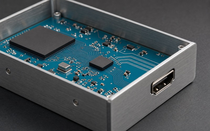
Start with the host display path
Confirm that the application processor can output the required image over MIPI DSI. The host needs a display controller, D-PHY transmitter, enough lanes, a supported pixel format and a timing generator that can produce the chosen mode. A processor with MIPI CSI camera input is not automatically able to generate DSI display output. Although LT9611UXC accepts DSI or CSI packet formats, an HDMI display product normally starts from a DSI-capable host display pipeline.
Record the host port, lane count, lane rate range, clock mode, burst or non-burst operation, color format and frame timing. Check whether the processor can split a high-bandwidth stream across two MIPI ports in the way expected by the bridge. Pin multiplexing and package options also matter. The bridge cannot repair an unsupported host mode, so the host and LT9611UXC configuration must be reviewed as one link before the schematic is frozen.
Keep the exact LT9611UXC identity
The material record should retain LT9611UXC in full, together with the approved product version and package. The Rev 1.4 brief lists U4, QFN64 at 7.5 by 7.5 mm and -40 to +85 degree C for the standard part. LT9611UXC-AU is separately identified as an automotive option qualified to AEC-Q100 Grade 3 testing. A purchasing description that omits the suffix and qualification record can mix devices that belong to different approval paths.
Silicon revision and firmware belong to the identity as well. Older product literature describes differences among earlier revisions, so a legacy board record should include the version originally validated. For a new design, use current manufacturer documentation and obtain the full specification, reference schematic, firmware release notes and programming procedure. Do not assume that an older code image or configuration table applies to every device marked LT9611UXC.
Calculate MIPI input bandwidth from the real mode
The product brief allows one or two MIPI ports, each with one clock lane and one to four data lanes. The stated 80 Mbps to 2 Gbps range is per data lane. Determine the required payload from active pixels, frame rate and bits per pixel, then include packet and blanking behavior for the selected DSI mode. A 4K60 label alone does not specify whether one port can carry the mode or whether a dual-port arrangement is required.
Use the actual host timing rather than a simplified resolution table. Packed RGB, loosely packed RGB and YCbCr formats consume different bandwidth. Burst mode can reduce the time spent transmitting active data, while non-burst operation follows a different timing relationship. Confirm that the host lane rate falls inside the bridge's supported range with margin at voltage and temperature. A calculation should be followed by measurement of the generated D-PHY stream.
Match color format and conversion behavior
LT9611UXC supports multiple DSI pixel encodings, including packed RGB and YCbCr options. The brief also describes RGB and YUV color-space conversion, with defined limits on the converted formats. Select one end-to-end path and document the host output, internal conversion, HDMI output encoding, color depth and chroma sampling. An accidental mismatch can produce incorrect colors even when the monitor locks to the signal.
Check the sink's accepted formats through its identification data and choose a mode the complete chain supports. A monitor may accept RGB at one timing but prefer YCbCr at another. Limited-range versus full-range interpretation can also change black and white levels. Use known test patterns for color bars, ramps, fine text and chroma detail during bring-up, and compare captured values rather than judging a colorful image by eye.
Separate current capabilities from older DSC references
Lontium's current Rev 1.4 brief describes the DSI/CSI receiver, color conversion and HDMI 2.0 transmitter without listing DSC decoding in its feature summary. Some older LT9611UXC literature includes revision-specific DSC statements. A design that depends on Display Stream Compression must therefore confirm the exact silicon version, firmware and supported slice or format constraints with Lontium instead of copying an older brief into a current requirement.
The safer baseline is to make the uncompressed lane and format budget work using the capabilities documented for the approved device. If compression is essential, treat it as a separately validated function. Exercise every resolution, color format and transition used by the product, and retain the manufacturer confirmation with the firmware release. A monitor displaying one compressed test stream does not establish coverage for the complete operating set.
Budget the HDMI output correctly
The HDMI transmitter is described as HDMI 2.0b, HDMI 1.4 and DVI 1.0 compliant, with TMDS data rates up to 6 Gbps and support for 4K at 60 Hz. The output budget still depends on pixel clock, color depth and chroma format. Deep color at a given resolution requires more TMDS bandwidth than 8-bit color, while YCbCr 4:2:0 can reduce the load for selected modes.
Confirm the exact timing against the sink and the HDMI rules rather than selecting 4K60 as a single undifferentiated mode. Include cable loss, connector discontinuity, ESD-device capacitance and board routing in the channel. The transmitter provides programmable swing and pre-emphasis, but those settings are tuning tools, not permission for a poor layout. Validate at the connector using the intended cable classes and representative sinks.
Plan audio together with video
LT9611UXC accepts I2S or SPDIF digital audio. The Rev 1.4 brief lists two-channel I2S from 32 to 192 kHz with 16 to 24 bit samples, while SPDIF supports PCM or compressed Dolby Digital and DTS streams up to a 192 kHz frame rate. Decide which interface the host can generate and which formats the product is licensed and expected to carry.
Clock relationships, mute control and stream changes need explicit handling. Test video mode changes with audio running, cable disconnect and reconnect, sink sleep, sample-rate change and application pause. Check lip synchronization over long playback. If the product does not need audio, define unused pins and firmware behavior rather than leaving the interface in an unknown state.
Define firmware ownership and update recovery
The bridge includes an internal microprocessor and embedded SPI flash for firmware and HDCP keys. It also provides a 100 or 400 kHz I2C slave interface, and the brief states that firmware can be updated through SPI or I2C. The product team must decide who supplies the image, how it is versioned, which host owns configuration and how a failed update is recovered.
Store the approved firmware checksum and configuration with the board revision. A production test should read back an identifying version and confirm that the expected mode starts from a cold power-on. Prevent ordinary application writes from reaching protected key or boot regions. If field update is required, design a recoverable sequence that tolerates power interruption and verifies the image before activation.
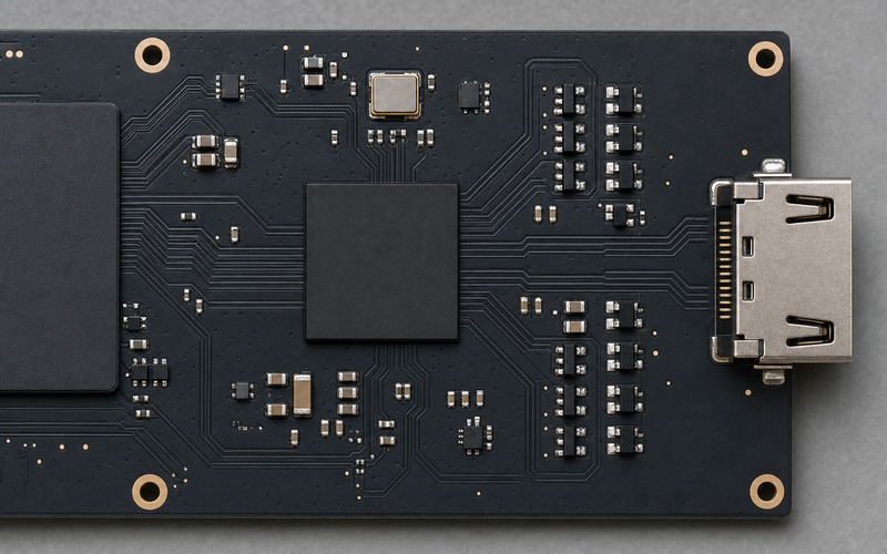
Handle HDCP and CEC as system functions
The product brief lists HDCP 2.2 and HDCP 1.4 support for output encryption. It also includes an integrated CEC controller but notes that command parsing is not included. These functions require policy, keys, firmware and host software beyond the electrical connection. Confirm licensing and key-provisioning responsibilities before enabling protected content.
CEC behavior should be limited to the commands the product actually supports. Test interactions with televisions, monitors, receivers and adapters because device behavior varies. Protected and unprotected video paths should both be verified across hot plug, sleep and mode changes. A missing or invalid key must fail in a controlled way without exposing unrelated configuration access.
Design the complete power and reset sequence
The short product brief does not provide the full rail list, current demand, ramp limits or reset timing needed for a schematic. Obtain the controlled specification and reference design before selecting regulators and level domains. The host I/O, bridge core, MIPI receiver, HDMI transmitter, oscillator and connector-side 5 V function may have different requirements. Use the exact limits rather than inferring supplies from a related Lontium device.
Analyze cold start, warm reset, cable insertion before host boot, brownout, watchdog recovery and orderly shutdown. Define pull states so HPD, DDC, CEC, reset and control pins do not back-power an unpowered domain. Place the required decoupling close to the QFN pads and verify rail noise while the link changes resolution. Firmware should wait for supplies and clock to stabilize before programming the bridge.
Place the QFN64 bridge between its two channels
The 7.5 by 7.5 mm QFN64 belongs between the MIPI source and the board-edge HDMI connector. Keep the MIPI groups direct from the host and the TMDS pairs short toward the connector. Place the external oscillator and specified load network close to the clock pins, then organize decoupling by rail. Avoid routing a switching regulator node or a high-current loop through either high-speed channel.
Build the footprint from the exact package drawing, including pin-one orientation, exposed-pad dimensions, solder-mask strategy, paste coverage and thermal-via requirements. The product brief gives the outline but not enough detail for a production footprint. Review the symbol, land pattern and escape together. An incorrect rotation can connect two visually similar differential groups to the wrong side of the device.
Route MIPI and HDMI as different high-speed interfaces
Both sides use differential signaling, but their electrical requirements and topology are different. Follow the host and Lontium rules for MIPI D-PHY impedance, pair matching, lane relationships and continuous references. On the HDMI side, control each TMDS pair, minimize intra-pair skew and preserve the reference plane through layer changes. Do not add test stubs to an active high-speed pair.
Keep pairs away from the oscillator, switching edges and connector 5 V path. Use symmetric via transitions with nearby return vias when layers change. Review the final stackup, copper thickness and fabrication tolerances with the board supplier. Automated length matching can create unnecessary serpentine coupling, so tune only to the limits required by the interface and simulation.
Put the HDMI receptacle and protection at the board edge
A cable connector must face outside the enclosure and remain mechanically accessible. The receptacle shell, anchoring tabs and board cutout should absorb insertion force without bending the QFN area. Keep the TMDS protection devices close to the connector and choose parts with capacitance suitable for the data rate. Route protection to a low-inductance return without forcing the high-speed pairs around long detours.
The HDMI interface also needs its connector-side 5 V function, hot-plug detection, display-data channel and CEC path implemented according to the full reference design and applicable interface requirements. Protect these lower-speed external lines from ESD and define their voltage domains. Connector shield bonding should follow the enclosure and EMC plan, with a deliberate path for cable discharge current.
Bring up the link in observable stages
Start by confirming every rail, reset and external oscillator. Then verify I2C communication and read an expected device or firmware identifier. Program a conservative known video mode, check MIPI activity at the input, confirm hot-plug and sink identification handling, and only then enable the HDMI transmitter. This order separates host, bridge and sink faults instead of changing several variables at once.
Capture register state and error information when a mode fails. A blank screen can come from absent DSI packets, unsupported pixel format, wrong lane mapping, unstable clock, failed sink negotiation, HDMI channel loss or protected-content policy. Keep a repeatable diagnostic mode with color bars and fixed audio. It should work without the AI application so display hardware can be tested independently.
Test across real sinks, cables and transitions
Use several monitors, televisions, capture devices, adapters and cable lengths. Exercise every supported resolution, refresh rate, color mode and audio format. Repeatedly connect and disconnect the cable, power the sink first and last, enter sleep, resume and change modes. Verify behavior at low and high ambient temperature and at supply tolerance.
Measure output quality with suitable high-speed equipment when the product's compliance target requires it. Watch for intermittent sparkles, link loss, audio dropouts, incorrect color range and slow recovery. Long tests matter because heat and repeated negotiation can expose problems a short bench image misses. Record the bridge firmware, host software, sink identity and cable used for each failure.
Treat an alternative bridge as a new interface design
A substitute must match more than MIPI input and HDMI output labels. Compare lane count and rate, single or dual-port mapping, DSI packet formats, color conversion, audio interfaces, HDCP generation, CEC behavior, control protocol, firmware method, package, power domains, temperature range and lifecycle status. Pin compatibility is uncommon and does not prove software compatibility.
If the exact LT9611UXC is changed, repeat the bandwidth calculation, schematic review, layout, firmware integration, sink matrix, EMC, ESD and compliance tests. Preserve the original board's validated firmware and configuration for service use. For a new platform, select a bridge with current documentation and direct support for the host and required output modes.
Complete the final video-bridge checklist
Before release, confirm the full LT9611UXC identity, U4 product version, QFN64 footprint, temperature requirement, host DSI mode, port and lane arrangement, pixel format, bandwidth margin, HDMI timing, audio path, firmware version, HDCP provisioning and CEC scope. Review every power rail, reset, oscillator, I2C access, decoupling group, MIPI pair, TMDS pair and connector-side protection function.
Qualification should cover cold and hot start, all modes, multiple sinks and cables, hot plug, sleep and resume, power interruption, firmware recovery, protected video, audio transitions, thermal equilibrium, ESD and mechanical insertion. A passing design produces the expected image and sound repeatedly while keeping its interface, security and recovery behavior controlled across production.