Free Shipping Over$200

- Products
- Marking
- Alternative

S29GL032A90TFIR40 as a Parallel NOR Flash
S29GL032A90TFIR40 as a Parallel NOR Flash
S29GL032A90TFIR40 is a legacy 32-megabit page-mode parallel NOR flash, equal to 4 MiB of nonvolatile storage. The original Spansion family information specifies a single 3.0 V supply, x8/x16 asynchronous operation, 90 ns initial access and 25 ns page access. The exact code identifies a lead-free industrial-temperature TSOP device with the R4 bottom-boot sector arrangement and tray packing.
This part belongs to a different design era from an eight-pin serial NOR. It presents address, data and control pins directly to the host, which can simplify memory-mapped reads but consumes many package pins and PCB routes. The 4 MiB array can hold boot code, FPGA configuration, fixed resources or service firmware in an established industrial controller where the processor already provides a compatible external memory interface.
A sound review starts with the existing board, processor bus, exact package drawing and released software. The 2005 source document carried an advance-information designation, so lifecycle and document revision require explicit confirmation before a new production commitment. Electrical similarity to a later S29GL family member does not prove a drop-in replacement. The checks below separate array organization, bus timing, update behavior, assembly and sourcing risk.
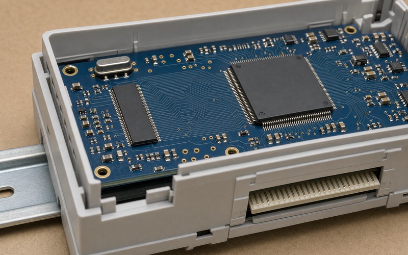
Decode the Full Orderable Code
Read the string from left to right. S29GL032A identifies the 32-Mbit MirrorBit page-mode family. The 90 speed option specifies a 90 ns random access class. T selects a standard-pinout thin small-outline package, F identifies the lead-free material set, I selects the industrial range from -40 to +85 degrees C, R4 selects the bottom-boot architecture, and the final 0 indicates tray packing in the original ordering table.
Keep the complete code in the schematic, bill of materials, approved-source list, programming definition and incoming inspection plan. S29GL032A alone does not define package, speed, temperature, boot-sector position or packing. The package marking may omit the packing character, so receiving inspection should reconcile the reel or tray label, purchase record and manufacturer marking convention instead of expecting every ordering character on the plastic body.
Decide Whether Parallel NOR Still Fits the Architecture
Parallel NOR offers direct, memory-mapped reads with separate chip enable, output enable and write enable controls. That can suit a processor or FPGA with an asynchronous external memory controller, especially in an established platform whose boot ROM already expects this interface. It also exposes enough pins for x8 or x16 data plus the address bus, control signals, power and ground, creating a larger package and a wider routing corridor than serial flash.
For a clean-sheet design, compare that board cost with a supported serial NOR, managed flash or newer parallel device before freezing the architecture. For a maintenance design, changing memory technology can force boot-code, timing, pinout and qualification changes that outweigh component savings. The correct question is whether the released host and recovery path depend on memory-mapped asynchronous behavior, not whether one interface appears newer.
Map 32 Mbit into the R4 Bottom-Boot Geometry
The 32-Mbit array contains 4,194,304 bytes or 2,097,152 sixteen-bit words. The R4 organization uses 63 main sectors of 64 KiB plus eight 8 KiB boot sectors at the bottom of the address space. Record byte and word addresses explicitly, because the host address presented in x16 mode and the byte address used by programming tools can differ by one address bit.
Place immutable startup code, recovery vectors and update metadata according to the processor's reset map and the physical bottom-boot sectors. Do not assume that a boot-sector variant can replace a uniform-sector or top-boot version merely because capacity and package match. Erase boundaries affect linker scripts, field updates, protection settings and production images. Verify the highest and lowest addresses in both bus-width modes.
Set x8 or x16 Mode Deliberately
The device can operate with an eight-bit or sixteen-bit data path. BYTE# selects the organization, and DQ15/A-1 changes role between word and byte modes. The schematic must show the intended state, host lane mapping and pull configuration. Firmware, debugger and programmer settings must use the same organization or words can appear byte-swapped, shifted or aliased even though basic reads return changing data.
Check endianness with a known pattern that exercises every byte lane, address transition and data bit. Include odd byte addresses in x8 mode and word-boundary transitions in x16 mode. If the board straps BYTE#, verify the strap at cold power-up and during reset. A floating or late-changing mode input can make a valid programmed image look corrupt before the application has any opportunity to diagnose it.
Treat 3.0 to 3.6 V as an Interface Requirement
The R4 ordering model operates from 3.0 to 3.6 V for read, program and erase. Verify the actual rail tolerance, host output-high and output-low levels, flash input thresholds and host input thresholds across temperature. A nominal 3.3 V label is insufficient when regulator tolerance, transient droop, connector loss and brownout behavior are included.
Keep CE#, OE#, WE#, RESET#, BYTE# and WP#/ACC in defined states while the supply ramps. The flash includes low-voltage write inhibition, but system design still has to prevent command-like transitions during unstable power. Check whether another powered device can drive the bus while flash VCC is absent. Back-powering through data or control pins can defeat reset assumptions and stress the interface.
Build the Read Timing Budget from 90 ns and 25 ns Limits
The 90 suffix represents the random address and chip-enable access class. Sequential page reads can use the internal four-word or eight-byte page buffer with a 25 ns page access after the first access. The host controller must distinguish first-access wait states from same-page page-mode timing. Crossing a page boundary returns the path to the longer access behavior.
Budget address setup, CE#, OE#, data valid, hold time, board delay and processor input setup at the slowest operating corner. Test isolated reads, sequential bursts and boundary crossings with caches disabled so the bus is actually exercised. Do not infer 25 ns random access from the page figure. Page-mode benefit depends on access pattern and controller support, and it disappears when software jumps frequently between unrelated addresses.
Route the Wide Bus as a Defined Interface
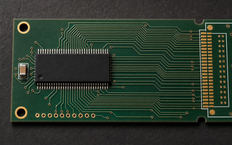
A practical x16 connection carries up to 21 address inputs, sixteen data lines and several controls. Reserve a continuous routing corridor between flash and host before placing unrelated circuits. Keep each signal over a reference plane, avoid long branches and minimize stubs at probes or test connectors. Group address, data and controls for review while preserving the pin escape required by the TSOP package.
Asynchronous does not mean edge-insensitive. Modern hosts can drive fast edges into a bus whose cycle time is much longer. Excess ringing can cross thresholds more than once around WE#, OE# or CE#. Use measured waveforms or simulation to decide whether source damping is needed. Validate the final drive strength, route stack-up, manufacturing tolerances and populated service connector rather than a simplified prototype only.
Control CE#, OE#, WE#, RESET# and RY/BY#
CE# selects the array, OE# controls read output and WE# qualifies command writes. Their overlap must follow the bus-operation table. RESET# should connect to a system reset path that returns the flash to read-array mode before boot fetches begin. RY/BY# can signal completion of embedded program or erase operations, while software status polling provides another route when the host lacks an interrupt input.
Review contention during direction changes. The host must release the data bus before the flash drives it, and the flash output must be disabled before the host begins a write. Check bus transceiver enable timing if one is present. A logic-analyzer trace should include address, representative data bits and all three strobes during boot, identification, word programming, write-buffer programming and sector erase.
Use CFI and Autoselect as Identification Evidence
Common Flash Interface data lets software discover capacity, command-set information and erase-region geometry. Autoselect provides manufacturer and device identification. Read both on the assembled board before erasing or programming. Store the expected values in the programming definition and reject an unknown response rather than applying a command sequence selected only from package appearance.
CFI compatibility does not make all parallel NOR devices equivalent. Sector protection, boot layout, reset behavior, command timing and package pinout can differ. The boot loader should return explicitly to read-array mode after any query or failed operation. Production tests should power-cycle after identification because a warm software reset can hide a missing hardware-reset connection or an incorrect power-on state.
Program with the Write Buffer and Verify Status
The family provides a sixteen-word or thirty-two-byte write buffer to reduce command overhead for multiword updates. Split transfers at the allowed buffer boundary, load the declared count and monitor Data# polling, toggle bits or RY/BY# until completion. A timeout must be based on documented maximum behavior and followed by status interpretation, reset and readback rather than an immediate blind retry.
Unlock-bypass and accelerated programming can improve factory throughput, but each adds procedure and fixture requirements. The high-voltage WP#/ACC path deserves its own electrical review and should never be improvised in field hardware. For normal in-system updates, prefer the simplest validated command flow that meets time limits. Verify every programmed range and preserve a hash or checksum tied to the released image revision.
Make Erase and Update Operations Survive Interruption
Main sectors erase in 64 KiB units, while the R4 bottom area provides eight 8 KiB boot sectors. Keep one verified startup path while changing application code. Write and verify the replacement region before switching an activation record. If the 4 MiB device cannot hold two full application images, retain a small protected recovery loader and a separate method for restoring the main image.
Test power removal during word programming, write-buffer programming, each sector type, protection changes and activation-record updates. On restart, the loader should decide from redundant integrity records rather than assuming the most recent command completed. Program Suspend and Erase Suspend can allow access to other sectors, but the software must define which reads and writes are legal while an embedded operation is paused.
Apply Protection to the Actual Boot Layout
The R4 model places the boot sectors at the bottom and defines hardware write protection for the bottom address region when WP#/ACC is low. Sector-group protection can lock additional areas. Map these mechanisms to the real reset vector, recovery code, factory constants and update policy. Test an operation that should fail and confirm the expected status response before relying on protection in service.
The Secured Silicon Sector provides a separate 128-word or 256-byte region that can be permanently locked. Decide at manufacturing time whether it holds identification data and who owns the irreversible lock action. Protection prevents accidental modification; it does not authenticate executable code. Signature verification, key storage and rollback controls remain separate system responsibilities.
Build the TSOP-48 Footprint from the Exact Drawing
The TFI R4 combination uses the 48-pin standard thin small-outline package. It has fine gull-wing leads along the two long sides, a clear pin-one convention and an exposed lead span that requires accurate pad length and solder-mask relief. Use the package drawing tied to the valid combination. A 48-pin TSOP from another memory family can have a different pinout even when the body dimensions look familiar.
Inspect first assemblies for lead coplanarity, bridges, insufficient wetting and package rotation. The long body can amplify placement and board-warp effects. Keep the CAD footprint, stencil aperture, assembly orientation and inspection criteria under revision control. The images in this guide show the package class and routing context; they are not dimensional land-pattern references.
Recheck Lifecycle Before a New Production Commitment
S29GL032A is a legacy family, and the source document used here dates from 2005 with an advance-information designation. That makes current lifecycle confirmation part of the engineering decision. Obtain the latest manufacturer status, change notices, last-time-buy information when applicable and an approved source plan before assigning the part to a new long-life platform.
For an existing product, preserve the exact released data sheet, approved ordering code and programmed image with the service record. Inspect date code, label structure and package marking against controlled references. Avoid inventory or delivery assumptions in the design approval. Purchasing evidence can change quickly, while the electrical and software qualification record must remain traceable for the product lifetime.
Qualify Replacements Beyond Capacity and Pin Count
A replacement must match voltage range, x8/x16 behavior, address map, 90 ns timing requirement, page-mode behavior, boot-sector location, command set, CFI geometry, protection, reset, standby current, package pinout and assembly constraints. A later S29GL032N family part may look related, but a family relationship is only a starting point for a difference table.
Run the released boot path, programmer and field-update procedure on every approved alternative. Cover random reads, same-page reads, page crossings, byte and word modes, high and low addresses, each erase-region type, suspend/resume, protection, reset and interrupted operations at voltage and temperature limits. Any mismatch needs an explicit hardware, software or manufacturing disposition before approval.
Make Production Programming Repeatable
The programming instruction should name S29GL032A90TFIR40, x8 or x16 organization, expected autoselect and CFI results, byte order, erase regions, image version, checksum, protection state and final read-array reset. Read identity before any destructive command. Program through a fixture whose voltage, pin mapping and bus direction have been verified against the assembled board.
After programming, read the complete image back through the product bus, power down until the rail discharges and perform a cold boot. Test the recovery entry and a protected-sector write rejection. Record programmer algorithm, adapter, fixture and image revisions. Socket programming evidence cannot replace an assembled-board test of power sequencing, bus timing, reset and address mapping.
Final Selection Checklist
Release the part only after the team has fixed the 4 MiB map, R4 bottom-boot geometry, x8/x16 mode, 3.0-to-3.6 V rail, 90 ns first access, 25 ns page timing, host wait states, address and data routing, control strobes, reset, CFI handling, erase strategy, protection, TSOP-48 footprint and recovery method. Keep the full ordering code in every controlled purchasing and manufacturing record.
On production-representative boards, verify cold and hot startup, rail limits, autoselect, CFI, low and high addresses, known data patterns, page boundaries, byte and word organization, write-buffer operation, main and boot-sector erase, suspend/resume, hardware protection, reset recovery, interrupted update and full readback. That evidence determines whether this legacy parallel NOR remains a dependable subsystem rather than a superficially similar memory part.