Free Shipping Over$200

- Products
- Marking
- Alternative

IS25WJ064F-JTLE-TR as a QSPI Flash
IS25WJ064F-JTLE-TR as a QSPI Flash
The IS25WJ064F-JTLE-TR is a 64-megabit serial NOR flash, equal to 8 MiB of nonvolatile storage. It belongs to ISSI's 1.8 V IS25WJ family and combines ordinary SPI with dual, quad and QPI transfers. The manufacturer selector lists a 1.65-to-2.0 V supply, fast-read operation up to 133 MHz for the family, an industrial temperature range from -40 to +105 degrees C, and compact 8-contact package choices.
This exact orderable part is useful when a low-power processor needs external boot code, FPGA configuration, fonts, audio prompts, calibration tables or a recovery image without the pin count of parallel NOR. The 8 MiB address space remains inside the range of three-byte addressing, which simplifies many boot paths. The low supply voltage creates a different integration problem: a 3.3 V host cannot be connected by assumption, even when the command set looks familiar.
A production design has to settle the full part number, rail tolerance, I/O voltage, reset state, quad-enable behavior, command set, dummy cycles, page and erase geometry, footprint and update policy together. Each item can break startup while the memory still passes a simple identification read. The following review treats the device as a board-and-firmware interface rather than a capacity line in a bill of materials.
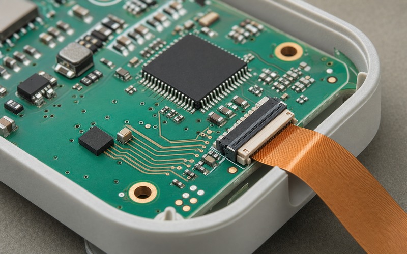
Decode the Full Orderable Part Before Layout
Keep IS25WJ064F-JTLE-TR as one controlled string in the schematic, bill of materials, approved-source record and programming instructions. The family name defines density and electrical behavior, while the suffix fixes package, temperature option, package content and tape-and-reel delivery. A shortened family name is useful for architecture work but is too vague for land-pattern release or incoming inspection.
The current product record identifies an 8-contact exposed-pad leadless package. Build the land pattern from the exact manufacturer package drawing tied to the suffix. Similar USON, UDFN and WSON labels do not prove the same body size, pad pitch, exposed-pad geometry or pin-one convention. Record the drawing revision beside the CAD library revision so a later package-table change can be reviewed instead of silently inherited.
Turn 64 Mbit into a Usable 8 MiB Map
A 64Mbit array contains 8,388,608 bytes. Start with explicit start and end addresses for the first-stage loader, main image, assets, calibration, factory identity, update metadata and recovery content. Leave room for image headers, signatures, version counters and erase alignment. An application binary that nearly fills 8 MiB leaves no realistic space for a second complete image or for growth across several product releases.
Separate frequently changed records from code. Calibration and user settings often need small updates, while firmware changes rarely. Put them in different erase regions and use sequence numbers plus integrity checks. If the product needs safe field replacement of a large image, decide early whether the flash can hold two slots. Otherwise, define an external recovery path rather than pretending spare space will appear later.
Use the 1.65-to-2.0 V Rail as a Hard Boundary
The IS25WJ064F family is a low-voltage device. Its supply range is 1.65 to 2.0 V, so it belongs on a controlled 1.8 V rail. Check the processor's VDDIO range for clock, chip select and all four data pins. A processor powered at 3.3 V may still have a separate 1.8 V I/O bank, but that must be configured and powered before it drives the flash.
When level translation is required, choose a translator that supports the direction changes and edge rates of quad I/O. Generic automatic bidirectional translators can distort clocked buses or fight during turnaround. Include translator delay in the timing budget and verify its power-off behavior. No signal may back-power the flash through an input clamp while the 1.8 V rail is absent or ramping.
Choose SPI, Quad I/O or QPI for the Actual Boot Path
Single-bit SPI is the simplest mode for identification, recovery and low-speed programming. Quad I/O moves read data on four lines while keeping a familiar command sequence. QPI can also move instructions and addresses on four lines, reducing overhead for repeated reads. The fastest mode is useful only if the boot ROM and later software agree on entry, exit, dummy cycles and reset behavior.
Measure the real workload. Loading one small configuration image at power-up may provide too little benefit for complex QPI state management. Repeated execution-in-place or asset fetches can benefit from quad transfers, but cache line size, random address changes and chip-select gaps reduce effective bandwidth. Keep a conservative single-SPI recovery procedure that can read identification and restore mode bits after an interrupted update.
Treat 133 MHz as a Board-Level Qualification Point
The ISSI selector lists up to 133 MHz for the fast-read class of IS25WJ064F. That number is an interface limit under specified conditions, not a promise that every board will boot at that clock. Useful throughput depends on command overhead, bus width, dummy cycles, controller pauses, receive sampling and any translator inserted between the host and flash.
Begin bring-up at a low clock. Read identification, SFDP data and known patterns, then increase speed while testing long and short transfers across page, sector and image boundaries. Repeat at rail limits and the intended temperature range. Save the controller's sampling point, drive strength and dummy-cycle setting with the validation record. Firmware changes to any of them deserve a new margin test.
Let SFDP Confirm Capabilities, Then Check the Exact Identity
Serial Flash Discoverable Parameters describe density, erase instructions and supported read modes in a machine-readable form. A driver can use them to avoid hard-coded assumptions that came from another flash family. The JEDEC identity still needs an allowlist. SFDP compatibility alone should not let an unknown device enter production or accept a software image built for different protection and reset behavior.
Some processor boot ROMs understand only a subset of SFDP or use fixed commands before the main driver runs. Verify the ROM's command, address width, quad-enable location and dummy-cycle expectation against this device's power-on state. If the ROM cannot recover from QPI or a changed volatile configuration, the application must leave the flash in the exact state expected at every warm reset.
Route Clock, Chip Select and Four Data Lines as One Interface
A quad connection has six timing-sensitive signals: SCK, CE# and IO0 through IO3. Keep them short over a continuous reference plane, avoid branches and limit unnecessary vias. The clock path often controls the margin because its edge rate is much faster than the nominal clock period suggests. Match data paths closely enough for the controller's sampling window rather than pursuing decorative geometric symmetry.
Place probes and production test pads so they do not become stubs on the fast bus. If damping is needed, choose the location and value from measurement or simulation. Validate with the final processor drive setting, final enclosure and representative production boards. A room-temperature read on one prototype cannot prove the interface at low voltage, cold startup and the upper operating temperature.
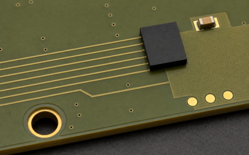
Place Decoupling at the Flash and Control Power Transitions
Put a local ceramic capacitor beside the flash supply and ground connections with a short return path. Check the 1.8 V rail's startup ramp, brownout threshold and load step when the processor and flash wake together. Chip select should remain inactive until the supply and host I/O bank are valid. Pull resistors must reference a rail that is present in every required power state.
Program and erase operations need a stable rail for their full duration. Before shutdown or deep sleep, stop new writes and poll the busy state. After an unexpected reset, do not trust previous volatile mode settings. Re-establish the required I/O mode, dummy cycles, protection state and deep-power-down state before the boot flow reads executable content.
Respect Page Boundaries and Erase Geometry
ISSI's serial NOR family programs up to 256 bytes per page and supports uniform sector and block erase choices such as 4 KB, 32 KB and 64 KB. Confirm the exact command table for this device and split every program transfer at a page boundary. A write that wraps inside a page can corrupt data while returning an apparently normal completion status.
Use 4 KB sectors for compact metadata and larger blocks for image replacement when that improves update time. Poll write-in-progress with a bounded timeout derived from guaranteed limits, then read back the changed range. The application should never erase a large block merely to change one counter. Small records need an append or rotation scheme that shares wear and survives interruption.
Build an Update Flow That Survives Power Loss
An update must preserve one verified boot path until the replacement image is complete. Write new data to an inactive region, verify the full hash or signature, then switch a small activation record stored in redundant copies. Do not erase the previous valid image until the new one has completed a cold boot and the product's functional checks.
If 8 MiB cannot hold two full images, use a smaller recovery loader that can fetch or reconstruct the main image through a separate channel. Test power removal during erase, during page programming and during activation-record changes. The recovery decision should depend on integrity records, not on the assumption that the last command probably finished before voltage disappeared.
Calculate Endurance from the Write Rate
The ISSI SPI NOR family is specified for more than 100,000 erase and program cycles and more than 20 years of retention. Those family figures still require a product calculation. A service counter updated every minute in one 4 KB sector can consume its cycle allowance much earlier than a firmware image written a few times during the product life.
Classify code, factory constants, event logs and user settings separately. Rotate high-write records across several sectors and include monotonically increasing sequence numbers plus integrity checks. Compare retention with the real temperature history, especially in sealed or outdoor products. A refresh procedure must keep a verified copy while rewriting instead of risking the only valid record.
Use Protection Bits with a Written Service Procedure
Serial NOR protection can prevent accidental program or erase of the loader, factory data or recovery region. Define which address ranges are protected after manufacturing and which software component may change them. Test one operation that should be rejected and record the expected status response. Protection that has never been exercised is only an assumption.
Document how an authorized update temporarily changes protection and restores it after verification. Flash protection is separate from authenticity. Signed images, key handling and rollback policy still matter when deliberate modification is in scope. The manufacturing station should read back the final protection state and store it with the programmed image revision.
Fit the 8-Contact Leadless Package to the Assembly Process
The JTLE-TR orderable part uses a compact 8-contact exposed-pad leadless package in the current product record. Hidden lands save area but remove the easy visual evidence provided by gull-wing leads. Land geometry, mask openings, paste apertures and the thermal or center pad must come from the exact package drawing. Do not substitute a generic 8-pin DFN library because the body looks similar.
Inspect first articles for rotation, insufficient wetting, bridges and voiding. X-ray or a qualified process coupon may be needed because the joints sit beneath the body. Keep the package drawing, footprint revision and stencil revision together in the manufacturing release. Incoming inspection should verify the complete suffix and reel label rather than checking only the IS25WJ064F family marking.
Make Production Programming Repeatable
A programming definition should name the exact part, expected identity, accepted SFDP response, erase map, image version, hash, clock rate and final protection state. Read identity before erasing. Program through the same voltage domain used in the product and avoid fixtures that drive 3.3 V into a 1.8 V interface.
After programming, read the full image back through the product signal path. Remove power completely, wait for the rail to discharge and perform a cold boot. Record the image, algorithm, adapter and fixture revisions for traceability. A socket programmer result is useful, but the assembled board still needs a test that proves its power, routing and boot-ROM assumptions.
Qualify a Second Source Beyond Density and Pin Count
Another 64Mbit QSPI flash can share the same eight signals and still fail as a replacement. Compare supply range, I/O thresholds, package drawing, power-on state, reset commands, quad-enable handling, SFDP revision, dummy cycles, page behavior, erase sizes, protection bits, deep-power-down timing and maximum current. Mark every mismatch with the owner who accepts it.
Run the released boot loader and update path on every approved source. Cover slow and fast reads, all used erase sizes, page boundaries, protection, sleep, brownout and interrupted updates at voltage and temperature limits. Keep source-specific parameters in controlled software data only when the boot ROM can tolerate the difference. Otherwise the replacement requires a hardware or boot-policy change.
Final Selection Checklist
Release the part only after the team has fixed the 8 MiB map, 1.65-to-2.0 V rail, host I/O compatibility, boot mode, clock, dummy cycles, page handling, erase strategy, protection, power-loss recovery, footprint drawing and programming method. The complete IS25WJ064F-JTLE-TR string belongs in every controlled record that can affect purchasing or assembly.
On production-representative boards, verify identity, SFDP, low and high addresses, continuous quad reads, cold and hot startup, rail variation, page programming, each used erase size, protection, deep sleep, reset recovery, interrupted update and cold boot after programming. That evidence is what turns a plausible QSPI flash choice into a dependable storage subsystem.