Free Shipping Over$200

- Products
- Marking
- Alternative

MT48LC8M16A2P-6A as SDRAM Working Memory for a Host
MT48LC8M16A2P-6A as SDRAM Working Memory for a Host
MT48LC8M16A2P-6A is a 128-megabit synchronous DRAM organized as 8M x16. That gives a host 16 MiB of volatile working memory on a sixteen-bit data bus. Micron's current catalog lists the -6A:L commercial-temperature version at 3.3 V, 166 MHz, CAS latency 3 and a 54-pin TSOP package. The catalog also lists an IT:L suffix for -40 to +85 degrees C. Those suffixes matter because the base name alone does not identify temperature range or the complete package and material option.
This device is working memory, not code storage that survives power removal. A processor can place frame buffers, network packets, audio windows, model activations, file-system cache and temporary application data in the SDRAM while it is running. Boot code still needs nonvolatile flash or another persistent source. The board therefore needs a host with a compatible classic SDR SDRAM controller, a clean 3.3 V interface, a clock and command bus, refresh support and enough pins for the multiplexed address and x16 data paths.
A successful design is shaped as much by timing and PCB layout as by capacity. The controller must initialize the array in the specified sequence, open and close banks correctly, issue refresh commands, obey delays between commands and keep the clock relationship valid at every receiver. The review below turns the part number into an implementable memory subsystem and shows where replacement risk enters before a board is released.
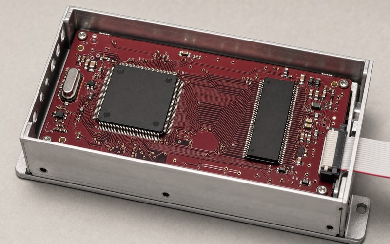
Start with the job assigned to working memory
Sixteen mebibytes can be useful in an MCU or embedded-host design that has outgrown internal SRAM but does not need a modern DDR interface. Budget memory by real consumers: display buffers, camera lines, protocol ring buffers, compressed assets, inference tensors, stacks and heaps. Include allocator overhead and the worst simultaneous operating mode. A nominal capacity match does not guarantee that latency, bandwidth or retention behavior fits the application.
SDRAM loses its contents when power is removed and depends on periodic refresh while powered. Brownout handling should stop new transactions, place the controller and memory in a defined state, and avoid treating stale data as valid after reset. Firmware should establish the SDRAM before any stack, heap or DMA descriptor is placed there. Recovery paths must still execute from internal memory or nonvolatile storage until the external array has passed a basic test.
Read the complete ordering code
MT48LC8M16A2P identifies Micron's SDR SDRAM family, the 8M x16 organization and the 54-pin TSOP style represented by P. The -6A speed grade is shown in Micron's current catalog at 166 MHz with CL3. The colon suffix remains part of the exact orderable identity. For example, -6A:L and -6A IT:L differ in operating-temperature qualification even though density, width and speed grade look similar.
The approved bill of materials should store the full manufacturer number, not a shortened search string. Incoming inspection, approved-vendor records and programming or board-test instructions should use the same suffix. When a distributor normalizes punctuation, compare the manufacturer's label and traceability record rather than assuming spaces and colons are cosmetic. A commercial-temperature unit is not automatically acceptable in an industrial-temperature assembly.
Translate 128 Mbit into the controller address map
The 8M x16 organization equals 134,217,728 bits or 16 MiB. Internally the array is divided into four banks, with row and column addresses multiplexed onto shared address pins. The controller therefore does not present a simple linear address to the package in one cycle. It activates a row in a selected bank, then issues a read or write with a column address and burst behavior defined by the mode register.
Document the host's byte address range, the SDRAM bank geometry and the conversion between processor bytes and memory words. Check whether the controller expects a specific row count, column count or bank count. A wrong geometry can appear to work in a small memory test yet alias high addresses onto lower locations. Test patterns must reach every bank, the highest row and column, and boundaries where the host changes bank or wraps a burst.
Confirm that the host has a true SDR SDRAM controller
A generic parallel memory interface is not enough. SDRAM requires a continuous clock relationship, encoded commands, bank state, refresh scheduling and mode-register programming. The host peripheral must support a 3.3 V single-data-rate SDRAM with a sixteen-bit bus and the part's geometry. Check the controller reference manual and validated board examples before assigning pins or assuming that an asynchronous external-bus controller can substitute.
Pin multiplexing is often the practical constraint. The design needs DQ0 through DQ15, address and bank lines, CLK, CKE, CS#, RAS#, CAS#, WE# and two DQM byte masks, plus power and ground. Confirm that those pins remain available with the selected display, camera, Ethernet, storage and debug interfaces. A pin conflict found after PCB layout can force a processor change rather than a memory change.
Treat 3.3 V as an interface contract
Micron lists these current -6A TSOP variants at 3.3 V. Verify the exact allowed VDD and VDDQ limits in the current data sheet used for the design, then include regulator tolerance, DC drop, ripple, startup and temperature. The host's SDRAM I/O bank must use compatible levels. A nominally 3.3 V processor pin is not proof that its absolute maximum, input threshold and output drive meet the memory interface under every rail sequence.
Avoid back-powering through address, command or data pins when either device is unpowered. The reset and power sequence should hold the host pins in a benign state until both rails and the clock satisfy their requirements. If the board has separate core and I/O rails, analyze every ramp and shutdown order. Measure the rail at the SDRAM pins during burst writes and refresh rather than relying only on the regulator test point.
Build the clock plan around the -6A speed grade
The current catalog identifies the -6A variant as a 166 MHz, CL3 device. That headline does not replace a timing table. The controller configuration must satisfy clock period, setup and hold times, row-to-column delay, precharge time, active time, refresh recovery and write recovery. If the board runs at a lower frequency, timing expressed in nanoseconds still has to be converted into a safe integer number of controller cycles.
CAS latency controls the delay from a read command to valid output data, but it is only one part of the access path. The processor may add arbitration, bus turnaround and cache refill delay. DMA traffic can keep banks open or cause repeated conflicts. Model the worst access pattern rather than quoting peak sequential bandwidth. A display or camera stream needs bounded service time, while inference scratch memory may care more about mixed reads and writes across banks.
Follow the power-up initialization sequence
After power and the clock become stable, the SDRAM controller must wait the required startup interval and issue the sequence defined by the selected Micron data sheet. The sequence normally brings CKE to the required state, precharges the banks, performs the required refresh operations and programs the mode register before normal traffic begins. Use the controller vendor's fields to express the actual device timing rather than copying unexplained hexadecimal values from another board.
Keep early startup code in internal memory until initialization and a short data test succeed. A debugger can mask errors by slowing the sequence or changing reset timing, so verify cold power-on without a probe. Repeat after short and long power interruptions, brownout and watchdog reset. Record the clock frequency and controller register values in the board configuration so a later firmware build cannot silently change the memory contract.
Understand bank activation and precharge
SDRAM access is stateful. An ACTIVATE command opens a row in one bank; a READ or WRITE then selects a column; PRECHARGE closes the row before another row in that bank can be opened. Auto-precharge can combine the close operation with a transfer when supported by the access pattern. Four banks allow useful overlap, but the controller still has to honor minimum active and precharge intervals.
Random traffic that repeatedly changes rows can lose much of the apparent bandwidth to activate and precharge cycles. Arrange frame buffers, packet rings and large arrays so common sequential work stays within useful row regions when practical. Do not optimize software around an assumed row size until the controller geometry is confirmed. Correctness comes first; bank-aware allocation is a measured performance refinement, not a substitute for valid timing.
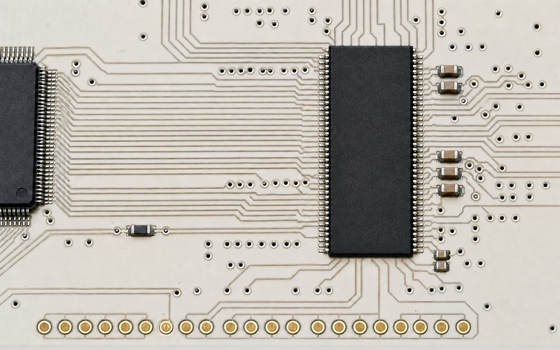
Program burst behavior and byte masks deliberately
The mode register selects burst length, burst order and CAS latency. Match these settings to the controller. A mismatch can produce repeated, shifted or truncated words while simple write-then-read tests still pass at some addresses. DQM controls the two byte lanes of the x16 interface, so byte writes and unaligned processor accesses depend on correct DQM routing and controller behavior.
Test full words, each byte lane independently, alternating patterns and unaligned accesses generated by the actual compiler and DMA engines. Check bus turnaround between reads and writes. If the processor uses cache, run both cached and uncached tests because cache hits can conceal a faulty external transaction. Logic-analyzer captures are most useful when correlated with the controller command sequence and the selected clock rate.
Keep refresh correct under every power mode
Dynamic cells must be refreshed even when application traffic is idle. Enter the row count and refresh interval from the exact data sheet into the controller, including the temperature conditions for the chosen suffix. Too little refresh eventually corrupts data; excessive refresh wastes bandwidth and power. Refresh must continue during ordinary idle periods unless the design intentionally enters a supported self-refresh mode.
Low-power firmware should distinguish clock gating, standby, self-refresh and complete power removal. Before changing CKE or the SDRAM clock, follow the controller and memory sequences. On wake, wait for the required exit timing before restoring traffic. Test long idle periods at temperature with memory patterns distributed across the whole array. A five-second bench test says little about a refresh error that develops after minutes or hours.
Route the bus as a timed synchronous interface
Place the single SDRAM close to the host and reserve a direct routing corridor before less sensitive nets occupy it. Keep the clock on a continuous reference plane, avoid plane splits and minimize unnecessary vias. Group command and address lines, route the x16 data bus as two byte lanes with their DQM signals, and control stubs. Classic SDRAM has no per-byte DQS strobe, so the relationship of every receiver to the common clock deserves explicit timing margin.
Length matching is a tool, not the whole solution. First reduce total flight time and topology discontinuities, then keep skew within the controller's board-level budget. Include package delay, output timing, input setup and hold, connector absence, temperature and voltage. Simulate or measure the clock edge, overshoot and settling on the final stackup. If series damping is needed, locate it according to the driver and topology instead of placing identical resistors by habit.
Give the rail a short high-frequency return path
Place small ceramic capacitors beside the SDRAM supply-pin groups with a short path to ground vias. Add local bulk capacitance for lower-frequency current changes and connect the region to a low-impedance 3.3 V distribution network. The controller, SDRAM and nearby interface loads can switch together, so calculate the rail with simultaneous activity rather than a single average-current number.
Ground pins need direct access to a continuous ground plane. Long necks, shared narrow traces and distant vias add inductance precisely where the interface needs a quiet reference. Probe with a short ground spring at the SDRAM side of the capacitors. Check startup, refresh, sustained writes and worst simultaneous I/O. A clean DC reading on a handheld meter cannot reveal fast droop or ground bounce.
Create the 54-pin TSOP footprint from the exact drawing
Micron's catalog identifies the P package as a 54-pin TSOP measuring about 10.00 by 22.00 by 1.20 mm for the listed -6A:L variants. Use the current package drawing tied to the exact suffix. The long body has fine gull-wing leads on the two long sides. Courtyard, pad length, solder-mask web, paste aperture and pin-one orientation must suit the assembly process and inspection method.
Check the first assemblies for bridges, insufficient wetting, bent leads, coplanarity and rotation. A visually similar TSOP from another SDRAM density may use a different address-pin function even when the outline matches. Keep symbol, footprint and schematic pin numbers under revision control. An approved land pattern does not prove electrical interchangeability; it only proves the mechanical interface was reviewed.
Choose the temperature suffix from the real enclosure
Micron's current catalog lists MT48LC8M16A2P-6A:L for 0 to +70 degrees C and MT48LC8M16A2P-6A IT:L for -40 to +85 degrees C. Select from measured component temperature, startup conditions and product qualification, not room ambient alone. A sealed controller near a display, regulator or processor can run materially hotter than the external air.
Temperature also reduces timing and power margin. Validate cold startup, hot refresh and sustained traffic on representative enclosures. If an industrial suffix is approved, keep that suffix in procurement and incoming inspection. Substituting the commercial suffix because the base name matches changes the qualification basis and requires engineering review.
Test more than a walking-bit pattern
A production memory test should cover data lines, address aliasing, bank selection, boundary crossings and retention. Use all-zero, all-one, alternating, pseudo-random and address-dependent patterns. Test each byte mask, uncached CPU access and the DMA masters used by the product. Fill the array, let it idle under normal refresh, then verify it after the longest relevant interval and at temperature.
Stress concurrent traffic that resembles the application: display reads while the CPU writes, network DMA while an audio buffer advances, or inference scratch access while storage is active. Monitor controller error flags and system resets. A failure log should capture clock, controller settings, rail voltage, board revision and temperature. Without that context, an intermittent timing problem can be mistaken for a software defect.
Qualify any replacement as a memory subsystem
Compare density, x16 organization, bank and row geometry, 3.3 V levels, speed grade, supported CAS latency, refresh requirements, command behavior, DQM, power modes, pin assignment, TSOP dimensions and temperature suffix. A part that fits the footprint can still require different controller registers or violate the existing timing budget. A faster headline grade does not automatically preserve every minimum and maximum timing relationship.
Build a difference table from current manufacturer documents and test the alternative on representative boards. Cover cold boot, warm reset, watchdog reset, sustained DMA, power cycling, idle retention and the full temperature range. Keep the approved manufacturer number and controller profile together. If software must detect variants, make the mechanism explicit; classic SDR SDRAM does not provide the rich discovery path expected from newer managed memories.
Use exact product records for suffix control
The verified internal product record for MT48LC8M16A2P-6A:L identifies the commercial-temperature TSOP option. A separate verified record covers MT48LC8M16A2P-6A IT:L. Both links were checked as live product-detail pages before this article package was prepared.
These records support part-number control; they do not replace the current Micron data sheet or a board qualification. Request the exact suffix on the quotation, confirm manufacturer traceability and compare the received label with the approved bill of materials. Keep availability and delivery decisions separate from the electrical approval.
Final SDRAM selection checklist
Confirm 16 MiB is enough, the host owns a compatible SDR SDRAM controller, the geometry is 8M x16 across four banks, and the I/O rail is valid at 3.3 V. Freeze the clock, CL3 setting and every timing field from the selected data sheet. Record initialization, refresh, CKE, mode-register, DQM and reset behavior in the board configuration.
Then verify the full suffix, temperature range, 54-pin TSOP footprint, routing topology, decoupling, startup and memory-test coverage. Exercise every bank and boundary with real DMA traffic at voltage and temperature limits. Approve alternatives only after the same electrical, firmware, assembly and traceability review. That process turns a familiar SDRAM number into reliable working memory rather than a capacity assumption.