 Free Shipping Over$200

- Products
- Marking
- Alternative

LM35 as an Analog Voltage Temperature Sensor
LM35 as an Analog Voltage Temperature Sensor
The LM35DZ/NOPB turns local temperature into an analog voltage with a nominal scale factor of 10 mV per degree Celsius. At 25°C the ideal output is 250 mV, and at 100°C it is 1.000 V. This direct Celsius calibration makes the arithmetic simple, but the finished measurement still depends on supply integrity, ADC reference accuracy, source settling, board temperature, wiring and mechanical placement.
Texas Instruments specifies the LM35 family for operation from a 4 V to 30 V supply and describes a drain current below 60 microamperes. The low current limits self-heating, yet it does not make placement irrelevant. A sensor beside a regulator, processor, display backlight or warm connector measures that local thermal field rather than the air, enclosure wall or process point named in the system requirement.
A useful design therefore starts with the quantity being measured and works backward. Define temperature range, response time, allowable total error, ADC range, cable length, electrical noise, condensation risk and calibration method before selecting the package and filter. The LM35 is simple at the pin level; extracting a trustworthy system temperature still requires a controlled analog and thermal path.
Translate output voltage into temperature
For a positive-temperature measurement in the basic connection, temperature in degrees Celsius is the measured output in volts divided by 0.010 V/°C. Firmware can apply the same relationship in integer units: 250 mV represents 25°C. Keep units explicit through the ADC conversion so that a millivolt value is not accidentally treated as volts or an ADC code as temperature.
The slope is the main conversion term, but offset and gain errors remain. A two-point calibration can estimate both if the product needs better system accuracy. A one-point adjustment corrects offset near that point but cannot distinguish sensor slope error from ADC reference gain error. Store calibration coefficients with units, valid range and test conditions.
Confirm package and pin orientation
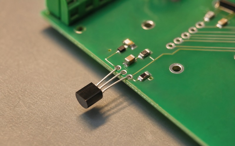
The selected LM35DZ/NOPB record uses a three-lead TO-92 package. The flat face is a useful assembly cue, but the controlled package drawing and pin table must define supply, output and ground. Transistor pin habits are unsafe because many TO-92 devices use different lead orders. Put pin numbers and the viewed side directly in the library review record.
Through-hole lead forming can rotate the body or stress the encapsulation. Specify insertion height, bend radius, board-side clearance and whether the body must extend beyond an edge or enter an airflow channel. Incoming inspection should check the complete orderable code and package, since another LM35 suffix can use a different body and assembly process.
Use the supply range with adequate margin
The 4 V to 30 V operating range does not mean every supply is equally useful. The lowest rail must still support the highest expected output, transient margin and any series protection. A 5 V analog rail is common, while a noisy switched rail may require local filtering. Verify the voltage at the sensor during startup, radio transmission and other worst-case load events.
Place a local bypass capacitor where the wiring or rail impedance warrants it. Keep the return short and do not route high-current pulses through the same narrow ground segment used by the sensor and ADC reference network. Supply ripple can appear as output error or excite the following sampling circuit even when average rail voltage is correct.
Design deliberately for temperatures below zero
The simplest single-supply circuit expects an output near ground at 0°C and cannot represent a negative voltage with a ground-referenced ADC. The datasheet provides full-range circuits that create a current path to a negative rail or otherwise shift the output. Select one of those methods when the specified minimum falls below 0°C instead of assuming software can recover a clipped node.
Check the complete low-temperature chain: sensor output compliance, bias resistor tolerance, negative source, ADC input range and startup behavior. If the product only operates above freezing, state that boundary in the electrical requirement and production test. A warm bench test cannot validate a cold-start corner.
Match the ADC reference to the signal span
A 0°C to 100°C span produces approximately 0 V to 1 V. Using a much larger ADC reference wastes codes and increases the temperature represented by one count. A lower reference or a suitable gain stage can improve resolution, but headroom, offset, input common-mode range and protection must be reviewed. Avoid adding an amplifier unless its errors improve the total budget.
Ratiometric behavior does not arise automatically because the LM35 output slope is not proportional to the ADC supply. Reference initial accuracy and drift therefore convert directly into gain error. Measure or specify the actual reference used by the conversion. A microcontroller label such as internal reference is not an accuracy statement.
Build a complete error budget
Include sensor initial accuracy and nonlinearity, long-term drift where relevant, ADC reference tolerance, ADC offset and gain, quantization, noise, leakage through protection parts, filter settling and calibration uncertainty. Thermal gradients and response lag belong in the same budget even though they are not electrical specifications. Express every item in degrees Celsius at the operating point.
Root-sum-square combination is reasonable only for independent random terms. Known limits, correlated reference errors and fixed thermal offsets may need worst-case addition. Keep a separate typical estimate for expected performance and a bounded acceptance budget for production. Do not use the typical curve as a guaranteed limit.
Control capacitive loading and ADC kickback
TI notes that the LM35 can directly drive about 50 pF without special precautions. Long traces, cables, connector capacitance and a switched-capacitor ADC can exceed that condition. The datasheet shows isolation and damping approaches using a series resistor or an RC network. Choose values from stability and settling requirements rather than adding a large capacitor at random.
The ADC acquisition capacitor must settle to the required fraction of a count during its sampling window. Check source impedance, multiplexer switching and sample rate. If channels with very different voltages are scanned, run a dummy conversion or extend acquisition time where the controller allows it. Confirm the result at temperature because leakage and amplifier behavior change.
Filter the signal without hiding real temperature changes
Temperature often changes slowly, so low-pass filtering can reject digital, motor and radio interference. Set the cutoff from the fastest legitimate thermal event and the required alarm delay. The electrical filter and the physical time constant of the package, airflow and mounting structure combine; a heavily filtered channel can miss a short overtemperature event.
Place the first filter element close to the ADC or at the cable entry according to the noise path. Keep high-impedance nodes short and clean. Verify step response with the real sensor mounting, not by injecting voltage only at the ADC pin. Voltage injection checks electronics but bypasses thermal lag.
Treat remote sensing as an analog interface
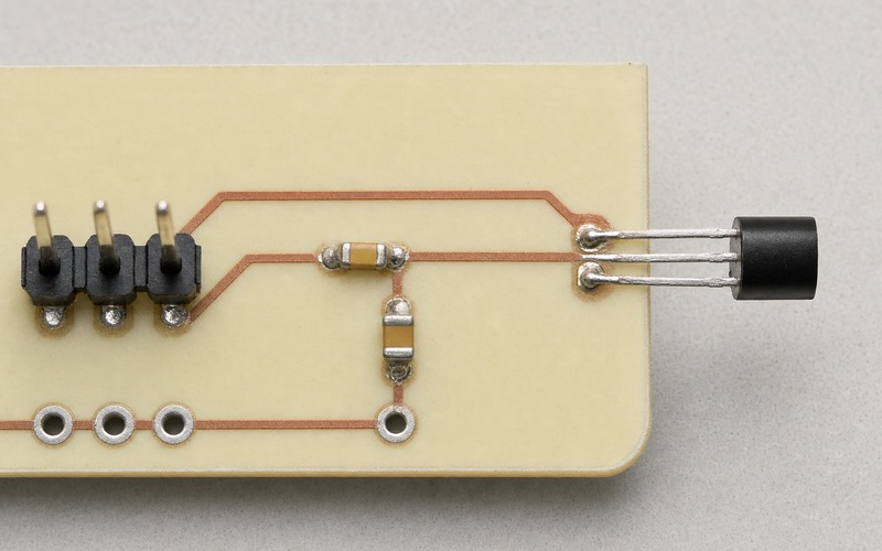
When the TO-92 device is remote, the supply, return and output conductors form an antenna and a resistance network. Use a defined cable, route the output beside its return and add protection appropriate to cable exposure. Ground drop from sensor current is small, but shared load current in the return can be much larger and directly shifts the reading.
Cable shields need a deliberate termination that matches the enclosure and EMC plan. Avoid connecting a shield in a way that carries power return current through the sensor reference. Test burst, RF and electrostatic events while logging raw ADC codes and recovery. A channel that survives but remains offset is not fully recovered.
Place the sensor at the real thermal target
For air temperature, extend the sensing body into representative airflow and reduce conductive heating through copper and leads. For board temperature, place it near the component or region of interest with a documented distance and copper connection. For enclosure temperature, define contact pressure, interface material and insulation from internal heat sources.
Keep the sensor away from regulators, processors, charging paths and LEDs unless those are the intended target. Board copper can conduct heat from distant parts. Use thermal testing and, where useful, a thermal camera to understand gradients. The drawing should control sensor height and orientation so production units reproduce the characterized geometry.
Account for self-heating and airflow
The low supply current gives low self-heating, with TI citing a small rise in still air. That advantage can be lost if external bias, contamination leakage or nearby copper carries heat into the package. Air velocity also changes the relationship between package temperature and ambient temperature. Compare still-air and forced-air conditions when both occur in service.
Do not pot or coat the body without measuring the resulting response and offset. Coating can improve environmental protection while adding thermal mass and coupling the sensor to the board. If protection is required, qualify the exact material thickness, cure and placement rather than accepting a generic coating process.
Define sampling, startup and fault behavior
A slow physical signal does not require uncontrolled firmware. Set a sample period, digital averaging window, plausibility range and timeout. Average after converting raw codes with a documented method, and retain enough raw information for diagnostics. Excessive averaging can delay alarms and conceal intermittent connections.
On startup, wait for the rail, reference and analog node to settle before accepting a reading. Detect open output paths, short-to-ground behavior and codes beyond the permitted temperature range. The LM35 has no digital fault register, so system diagnostics must infer wiring faults from circuit behavior and, where needed, added test components.
Calibrate the assembled signal chain
Calibration should include the sensor, wiring, ADC reference and mechanical placement. Use traceable temperature points with sufficient soak time and a reference probe placed at the same thermal target. Record chamber stability and gradients. Moving a reference probe closer to the air stream than the product sensor creates a comparison error.
Choose calibration points around the range that matters. A two-point correction supports slope and offset; more points can characterize nonlinearity but increase test time and data management. Recheck a sample across temperature after coefficient quantization in firmware. Production limits should include reference uncertainty and repeatability.
Protect the input without adding hidden error
Series resistance, clamps and filters can protect a cable-connected ADC, but leakage and resistance interact with the LM35 output and sampling network. Select low-leakage parts for the temperature range and evaluate them after humidity and surge stress. A protection device that looks open at room temperature may create measurable error when hot.
Route surge current to a robust return before it reaches the quiet analog ground. Keep the sensor output away from fast GPIO, switching inductors and clock lines. Review connector pin order so supply or external voltage cannot be applied to the output during mis-mating. Fault tests should cover powered and unpowered states.
Control identity and production test
Maintain the full LM35DZ/NOPB code, approved manufacturer, package drawing and marking reference in procurement records. Visual similarity to another TO-92 temperature part does not establish the same scale factor, pinout or range. Verify source documentation and apply risk-based incoming inspection without making assumptions from body shape alone.
A production test can measure rail current, output at a controlled temperature and ADC conversion. A single ambient point catches gross pin, assembly and offset faults; a second controlled point verifies slope when the product risk supports it. Keep fixture self-heating and airflow consistent so the test does not create its own temperature shift.
Complete the LM35 channel checklist
Before release, confirm the exact suffix and TO-92 pinout, 4 V to 30 V supply condition, required temperature range, below-zero circuit if applicable, 10 mV/°C conversion, ADC reference, acquisition time, filter values, capacitive load, cable protection and fault thresholds.
Then review sensor location, airflow, conductive heat paths, coating, response time, calibration points, firmware units, raw-code logging and production test. The best LM35 circuit is a short schematic backed by a precise thermal and measurement definition.
Related information
- 2026.07.17 TMP102 for Low Cost Board Temperature
- 2026.07.17 TMP117 for High Accuracy Digital Temperature
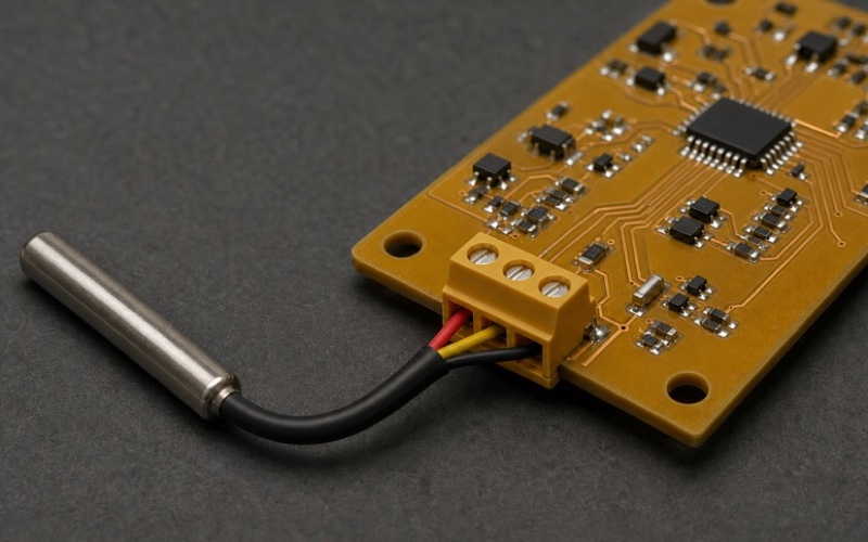
- 2026.07.17 DS18B20 on a One Wire Temperature Bus
- 2026.07.17 VS1011E as an Integrated MP3 Audio Decoder


