 Free Shipping Over$200

- Products
- Marking
- Alternative

VS1011E as an Integrated MP3 Audio Decoder
VS1011E as an Integrated MP3 Audio Decoder
VS1011E combines an MPEG audio decoder, a programmable DSP core, serial control logic, a variable-sample-rate stereo DAC and an earphone amplifier in one device. It accepts compressed audio through a serial data interface, decodes the stream, applies digital volume and tone controls, and produces left and right analog outputs. That integration can simplify a compact player, annunciator or embedded audio terminal, but the chip still depends on a host, clean power, a valid clock and a carefully designed output path.
The official datasheet lists MPEG 1.0 and 2.0 Layer III support for constant, variable and average bit rates. WAV PCM and IMA ADPCM are also supported, while Layer I and Layer II decoding require separate activation. VLSI Solution marks the device discontinued. Existing equipment therefore needs exact identification and controlled maintenance, while a new design should compare supported formats, software effort, power rails, package and analog behavior with a current decoder.
Separate the decoder from the storage controller
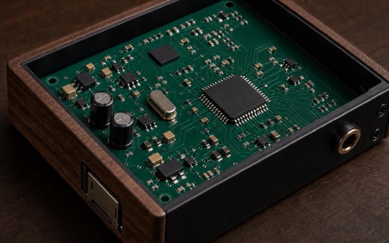
A microSD socket beside VS1011E does not mean the decoder contains a native SD-card controller. In the usual slave arrangement, a microcontroller reads sectors, parses the file system or streaming source, and feeds compressed bytes to the serial data interface. The decoder handles the audio bitstream after those bytes arrive. Storage initialization, directory handling, file selection, buffering and user controls remain host responsibilities.
This boundary should be visible in the schematic and firmware architecture. Give the card its own chip select and route it to the host. Give VS1011E separate control and data selects according to the selected SPI arrangement. Size host buffers for storage latency, filesystem work and other interrupt activity. A player that works with one card on a quiet bench can still underrun when erase blocks, display updates or communications delay the next read.
Confirm LQFP-48 or SOIC-28 before layout
VS1011E appears in both LQFP-48 and SOIC-28 packages. The two packages differ in pin count, footprint, exposed signal set and routing opportunities. A board drawing that shows a square 48-lead package cannot be used to approve a long 28-lead footprint. Keep the complete orderable identity, package drawing, pin-one indicator and land pattern together in the controlled component record.
The LQFP form gives access to more pins and provides routing around four sides. The SOIC form can suit a simpler assembly but concentrates connections on two edges. Review the official pin table for the exact package before assigning every net. No-connect pins, test functions, boot straps and supply pins need the stated treatment even when a previous family member used a similar name.
Use SCI for control and SDI for audio data
The Serial Command Interface, or SCI, reads and writes 16-bit control registers. A transaction contains an instruction byte, an address byte and one data word. The Serial Data Interface, or SDI, carries MP3 or WAV bytes into the decoder. Treating these as one undifferentiated SPI peripheral often produces chip-select mistakes and control words inside the audio stream.
VLSI Solution documents several ways to connect the buses, including shared signal arrangements. Select one official topology and reproduce its chip-select logic exactly. Keep the controller driver explicit about whether each transfer targets SCI or SDI. Logic-analyzer captures should show idle levels, clock edge, select timing and byte order at the decoder pins rather than at a distant header.
Let DREQ govern every transfer burst
DREQ is the decoder's flow-control signal. When DREQ is high, the datasheet states that VS1011E can accept at least 32 bytes of SDI data or one SCI command. When it is low, the sender must stop starting new data. Firmware that waits for DREQ once and then transmits an unlimited file block can overrun the input path.
DREQ can change during a byte. The host should finish the byte already in progress, then use the signal to decide whether another transfer may start. A practical driver sends bounded bursts and checks DREQ between them. Test this behavior at low bit rates, high bit rates, file transitions, bass enhancement settings and simultaneous host activity because decoder consumption is not constant in every state.
Choose a clock that preserves sample-rate accuracy
VS1011E operates from a nominal 24.576 MHz master clock. That clock can be supplied directly, or a 12.288 MHz crystal or external source can use the internal doubler. The datasheet accepts input clock ranges around 12 to 13 MHz with doubling and 24 to 26 MHz without it. A 12.288 MHz crystal is a natural audio choice because doubling reaches 24.576 MHz.
Set SCI_CLOCKF before audio decoding when the input differs from the reset assumption. The master clock affects the sample-rate converter, supported audio workload and SPI timing limits. A convenient processor oscillator with the wrong frequency can shift playback pitch. Verify crystal load capacitors, startup margin and measured frequency on the assembled board, then confirm output sample rate with a known test stream.
Keep analog and digital supplies within their domains
The device uses separate analog and digital supply pins. The official operating table places the analog domain from 2.5 to 3.6 V. The digital minimum depends on whether the clock doubler is active, with the doubled-clock condition requiring the higher minimum stated by the manufacturer. A casual 5 V connection is outside the device supply limits.
Place local bypass capacitors beside each supply pin and give them short return paths. Keep card-socket current, host clock return and decoder digital current away from the DAC reference and output area. If separate regulators are used, define their startup behavior and common ground path. Probe both rails while decoding a demanding file and while the storage interface is active, since a quiet idle measurement can hide dynamic coupling.
Plan reset, boot straps and startup order
Hardware reset places the analog and digital sections in a low-power state and stops the clocks. After reset releases and DREQ indicates readiness, the host can configure mode, clock, tone and volume registers. Audio bytes should not start before the device is ready. Reset duration and the relationship between supply rise, clock startup and DREQ deserve explicit firmware timing.
Some pins participate in SPI boot or mode selection. Their pull resistors determine whether the device attempts an external boot. Use the values and directions from the selected package connection diagram. During board bring-up, inspect reset, crystal activity and DREQ first. A silent output caused by an unintended boot strap can otherwise look like a codec or analog failure.
Design the stereo output as an analog circuit
The integrated DAC and earphone amplifier can drive a 30 ohm load under the stated conditions. Left, right and common-buffer behavior still require the recommended connection method. The output is not a generic pair of ground-referenced power-amplifier nodes. Headphone, line-output and externally grounded equipment present different return and protection requirements.
Follow the official analog-output note for AC coupling, common-buffer use, ESD protection and line-output conversion. Keep output traces short and symmetric. Place protection close to the outward-facing jack, while preserving the intended load and frequency response. Test with the real headphone impedance, cable capacitance and external amplifier input that the product expects.
Protect the jack without degrading audio
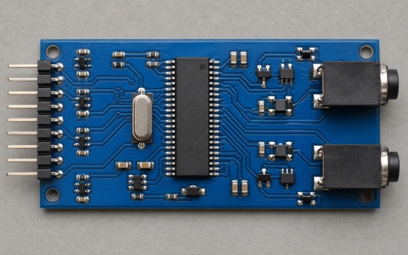
An exposed 3.5 mm connector brings electrostatic discharge and cable transients directly to the audio section. Protection devices need low enough capacitance and suitable clamping behavior for the signal level. Their return path should reach the intended chassis or circuit reference without sending the event through the decoder ground network.
Series resistance, coupling capacitance and any common-buffer network affect low-frequency response and load drive. Calculate the high-pass corner with the minimum expected load. Measure channel separation, output noise, distortion and pop energy with the protection components fitted. A circuit validated before the final jack and enclosure can produce different results after those mechanical parts are added.
Budget host bandwidth and buffering
A 320 kbit/s MP3 stream averages 40 kB/s before filesystem overhead, which is modest for many controllers. Average rate does not describe burst timing. The host may pause for card reads, metadata parsing, display service or network traffic, while VS1011E continues consuming compressed data. A software buffer should absorb the longest credible service delay.
Record buffer fill level and DREQ behavior during stress testing. Exercise high-bitrate files, variable-bitrate transitions, damaged headers, short tracks and rapid track changes. The host should recover from a card read error without sending unrelated memory into SDI. Define a controlled cancel or end-fill procedure so one file does not contaminate the next decoder state.
Validate codec and container assumptions
The product name emphasizes MP3, but a file extension does not prove that its contents match a supported stream. Verify MPEG version, layer, sample rate, channel mode and bit rate. WAV support applies to listed PCM and IMA ADPCM forms, not every codec that can be stored inside a RIFF container. Optional MPEG layers also need the documented enabling method.
Build a qualified media set with constant, variable and average bit rates, mono and stereo content, supported sample rates and boundary cases. Include malformed or truncated files to confirm that the user interface stays responsive. Check decoded sample rate and channel assignment rather than relying on audible output alone.
Control volume, tone and mute behavior
SCI_VOL provides independent channel attenuation in 0.5 dB steps. The reset state is full volume, so the host should write a safe operating value before enabling the external path. Bass and treble settings consume processing margin and change spectral output. Store limits that match the headphone stage, enclosure and connected amplifier.
Define mute behavior for power-on, track changes, data loss and shutdown. Digital attenuation alone may not suppress every transient from rail sequencing or jack insertion. Measure startup and shutdown at the connector with a representative load. If an external mute switch or amplifier is present, coordinate its timing with reset, clock readiness and decoder configuration.
Lay out the board around current paths
Place the crystal and its load components close to XTALI and XTALO. Keep those traces compact and away from the analog outputs. Position supply capacitors at their pins, then route SCI and SDI between the host and decoder without crossing the quiet output region. The microSD socket belongs at the board edge with short host connections and a mechanically accessible insertion direction.
VLSI Solution's layout guidance favors a coherent ground structure and careful separation by placement rather than long return detours. Review where card current, host current, decoder digital current and headphone current close their loops. The jack opening, storage opening and any shield contact should face the enclosure wall, not the center of the PCB.
Measure more than successful playback
Functional testing should confirm reset, register access, DREQ response, sustained SDI transfer, clock frequency and supported file decoding. Analog testing should cover output level, frequency response, noise, total harmonic distortion, channel separation and load behavior. Run these checks from minimum to maximum permitted supply and over the product temperature range.
Monitor the output during card access, host radio bursts, display updates and processor load changes. Listen for periodic tones, but also inspect the spectrum because low-level coupling can be hard to hear. Verify that the left and right channels remain in phase and that volume commands affect the intended channel.
Treat replacement as a system migration
VS1011E is discontinued, and a current decoder can differ in supported formats, register map, patches, clocking, supply voltages, package, GPIO, output common mode and headphone capability. Pin similarity does not establish software or analog compatibility. Migration should compare the complete data path from storage and host firmware through to the connector.
Capture the existing SPI traces, register initialization, clock measurement and analog performance before changing hardware. Then qualify the candidate with the same media and electrical tests. A successful migration preserves required user behavior while documenting every schematic, layout, firmware and production-test change.
Complete the VS1011E design review
Before releasing a board, confirm the exact package, official pin table, power limits, clock source, reset timing, boot straps, SCI and SDI selects, DREQ handling, host buffer size and supported media set. Verify that the host, rather than the decoder, owns the microSD interface and file system.
Review bypass placement, ground returns, crystal routing, jack protection, common-buffer connection, load impedance, startup volume, mute timing and end-of-stream handling. For existing products, add lifecycle and incoming-identity controls. These checks turn the integrated decoder into a predictable audio subsystem instead of a part that merely produces sound on a prototype.
Related information
- 2026.07.17 LM35 as an Analog Voltage Temperature Sensor
- 2026.07.17 TMP102 for Low Cost Board Temperature
- 2026.07.17 TMP117 for High Accuracy Digital Temperature
- 2026.07.17 DS18B20 on a One Wire Temperature Bus


