 Free Shipping Over$200

- Products
- Marking
- Alternative

TMP117 for High Accuracy Digital Temperature
TMP117 for High Accuracy Digital Temperature
TMP117 is a factory-calibrated local digital temperature sensor for designs where fractions of a degree matter. According to the official TI product page, the device combines a direct digital result, I2C and SMBus compatibility, programmable limits, low current consumption and nonvolatile memory. Those features remove much of the analog signal-chain work associated with a platinum RTD, but they do not remove the thermal design problem. The silicon reports the temperature that reaches its own die. Accuracy at the die can be excellent while the system result is wrong because heat arrived from the regulator, the processor, the enclosure or the wrong side of the board.
The TMP117 data sheet specifies a maximum error of ±0.1°C from -20°C to 50°C, ±0.15°C from -40°C to 70°C, and progressively wider limits toward the full -55°C to 150°C operating range. Its 16-bit result uses 0.0078125°C per least significant bit. Resolution is therefore much finer than guaranteed accuracy. A stable sequence of codes does not prove that the sensor has reached the temperature of the intended object.
A successful design begins by naming the measurement target. Ambient air, a metal surface, a fluid path, skin contact and the local PCB region require different thermal paths. The copper, board thickness, solder joints, package pad, nearby components and airflow determine which temperature dominates the result. The electrical interface is straightforward compared with that thermal network.
Start with the required accuracy over the real temperature range
The headline ±0.1°C limit applies from -20°C to 50°C. A design that must operate beyond that interval has to use the applicable limit: ±0.15°C from -40°C to 70°C, ±0.2°C from -40°C to 100°C, ±0.25°C from -55°C to 125°C, or ±0.3°C from -55°C to 150°C. Put the full environmental range in the requirement before assigning the remaining error budget.
The sensor specification is one contributor. Thermal offset between the target and the package, self-heating, enclosure gradients, mechanical stress, power-supply sensitivity, reference-instrument uncertainty and test-fixture repeatability also contribute. These terms should be estimated separately. Treating the digital code width as total measurement uncertainty produces an unrealistic budget.
TI states that production units are tested on a NIST-traceable setup verified with equipment calibrated through ISO/IEC 17025 accredited standards. Traceability supports calibration records, yet it does not transfer through an unknown system thermal path. A finished product still needs verification against a suitable reference in its assembled mechanical condition.
Choose the package and the thermal contact together
TMP117 is available in a six-pin 2.00 mm by 2.00 mm WSON and a smaller six-ball DSBGA. The WSON is convenient for conventional assembly and gives the layout engineer a defined exposed-pad area. The DSBGA reduces area and thermal mass but places tighter demands on assembly capability, inspection and board finish. Package choice affects response time and the direction through which heat reaches the die.
For a rigid PCB, TI recommends leaving the WSON thermal pad unsoldered when high precision is required without system calibration. Soldering that pad can improve thermal coupling to the board and shorten response, but package stress can add measurement error. If the pad is soldered, it must be left floating or connected to ground. A standard reflow process is preferred because manual soldering can introduce additional stress.
That guidance is application dependent. A sensor intended to follow a solid surface benefits from low thermal resistance to that surface. A sensor intended to read air needs reduced conduction from unrelated board heat. Decide which path deserves low resistance, then suppress competing paths.
Build a thermal island for ambient or probe measurements
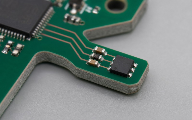
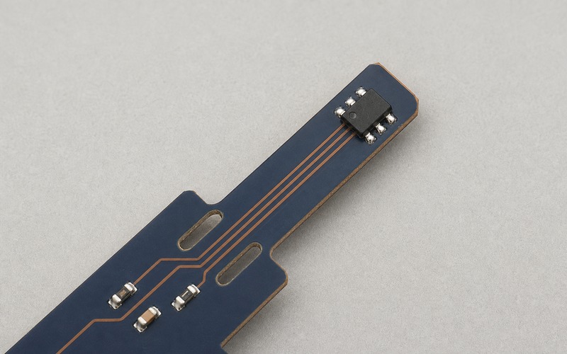
The TI PCB temperature-sensor layout report explains that a routed slot or partial cutout around a sensor reduces heat flow through FR4. An island supported by a narrow neck can separate the sensing region from processor and power heat. Thin traces carry power and digital signals across the neck while limiting copper conduction.
Keep solid ground pours, wide power copper and internal planes from bridging the thermal moat. A visually isolated top layer can remain thermally coupled through buried copper. Review every layer and the copper balance around the island. Stitching vias beside the sensor would also create an efficient thermal path back to the main board, so use them only when that coupling is intended.
Place the isolated region where the target medium can reach it. For air measurement, a vent path and realistic board orientation matter. A sensor hidden behind a warm display, a sealed battery pocket or a stagnant internal cavity measures that local microclimate. The enclosure model should define inlet area, airflow direction and shielding from radiation produced by hot internal surfaces.
Keep local heat sources away from the sensor
The sensor itself consumes little power, but nearby pullup resistors, LEDs, oscillators and regulators can create a larger offset than the intrinsic error limit. TI specifically warns that pullup resistors can act as heat sources. Put the I2C pullups on the main board side of the thermal neck and route the two signals to the island.
Do the same with the bypass network where practical while keeping the required 100 nF capacitor close to the supply and ground pins. The capacitor is electrically local and thermally small. Large resistors, indicator devices and power filtering parts belong farther away. Use narrow, symmetrical copper connections that meet current and signal requirements without forming a thermal strap.
Radiated and convective heat can bypass a well-designed moat. A hot processor facing the sensor across a small enclosed gap can still bias the reading. Move the sensor out of that view, add a suitable internal shield, or change airflow so the target medium reaches the sensor before it passes over the heat source.
Control self-heating with conversion timing
TMP117 typically consumes 3.5 µA with a 1 Hz conversion cycle and no averaging. Active conversion current is much higher for a short interval, and more averaging increases active time. TI lists a typical conversion time of 15.5 ms for one conversion. Eight samples therefore keep the converter active for about 124 ms before the result is reported.
In a documented still-air example on a small coupon at 3.3 V, continuous operation without a standby interval produced about 40 m°C of self-heating at 25°C. That value belongs to the stated setup rather than every PCB, but it demonstrates that tens of millidegrees matter when the total target is a tenth of a degree.
Use one-shot mode or a conversion cycle with meaningful standby time when the application permits it. TI describes eight-sample averaging with a one-second cycle as a practical balance in many cases because the inactive interval lets the device cool. The minimum acceptable supply voltage, larger pullups and limited bus traffic further reduce dissipation.
Use averaging for noise, not for thermal error
The device supports averages of 1, 8, 32 or 64 conversions. Averaging reduces code variation when the measured temperature changes slowly and the supply is stable. TI reports repeatability of roughly ±3 codes without averaging and about ±1 code with eight averages in its characterization discussion.
Averaging cannot correct a sensor that is thermally coupled to the wrong object. It can make a biased reading look more stable. Begin with a layout and mechanical path that bring the die toward the target temperature, then select enough averaging to meet display, control or logging noise requirements.
Higher averaging also lengthens active conversion time and raises average current. A slow environmental logger may prefer one measurement followed by shutdown. A control loop may need a shorter cycle and less averaging. Record the selected mode, cycle and average count as part of the measurement specification.
Read the 16-bit result correctly
The temperature register is a signed 16-bit two's-complement value with 0.0078125°C per code. Convert the received most-significant byte and least-significant byte into a signed 16-bit integer before multiplying by the scale factor. Performing an unsigned conversion first breaks negative temperatures.
After reset, the register reads the reserved -256°C code until the first conversion, including the configured averaging sequence, is complete. Firmware should use the data-ready indication or allow the documented conversion time instead of accepting the reset value as a measurement.
Test the conversion routine with positive, near-zero and negative patterns. Include the exact boundary between 0x0000 and 0xFFFF. Log raw codes during validation so a byte-order or signedness error is visible without interpreting formatted decimal output.
Design the I2C connection for four possible addresses
ADD0 can connect to ground, the supply, SDA or SCL, selecting addresses 0x48 through 0x4B. Up to four devices can therefore share one bus without an external address translator. Tie ADD0 directly to the intended node and make the connection clear in the schematic and assembly documentation.
SDA and ALERT are open-drain. SCL also needs a pullup when the controller uses an open-drain clock output. TI shows 5 kΩ as a typical value and recommends avoiding values below 2 kΩ when self-heating matters. Calculate pullups from bus capacitance, rise-time limits, logic levels and total low-level sink current rather than copying one value across every board.
The interface supports clock rates from 1 kHz to 400 kHz. Faster transfers can reduce the time that digital input cells and pullups dissipate power, but bus length and capacitance still limit the useful speed. Keep routing away from noisy switch nodes and avoid heavy unrelated traffic when a precision conversion is being taken.
Use alerts as a controlled system function
Programmable high and low limits let ALERT drive a controller interrupt or an SMBus alert line. Define whether the output represents a temperature threshold, data-ready state or another configured function. Confirm polarity and clearing behavior in firmware and test both rising and falling boundary crossings.
A thermal protection function needs an independent response path analysis. Consider sensor location, conversion latency, averaging delay, controller interrupt latency and actuator response. A precise steady-state sensor does not guarantee fast protection if a high thermal mass or long cycle hides a rapid event.
If ALERT is unused, TI allows it to float or connect to ground. Leaving it as an unreviewed test point can introduce leakage or noise. Give every pin an intentional state in the production design.
Use the EEPROM carefully
TMP117 includes 48 bits of general-purpose EEPROM and nonvolatile configuration capability. The EEPROM is locked by default to reduce accidental programming. Unlocking, writing, waiting for completion, resetting and reading back form a controlled programming sequence.
TI programs a unique identifier in general-purpose EEPROM locations to support NIST traceability and warns that reprogramming those locations removes that function. Decide whether the application needs the factory traceability information before allocating the memory. Do not use the EEPROM as a frequently updated event log because programming has finite endurance and adds current.
Manufacturing software should verify every programmed value after the general-call reset loads nonvolatile settings. Field firmware should distinguish volatile configuration changes from intentional EEPROM programming so a transient command cannot alter the power-up state.
Apply digital offset after measuring the assembled system
The digital offset register can correct a repeatable system shift. Use it after the thermal construction is stable and the product has been compared with a calibrated reference. An offset taken on an open bench can be wrong after the board is installed in an enclosure.
Measure at multiple points across the intended range. A constant offset can correct a nearly parallel error, while a temperature-dependent slope or long settling time points to a thermal-path or method problem. Do not conceal a strong gradient, poor contact or inconsistent assembly with a single correction number.
Store calibration conditions with the result: reference sensor, immersion depth or contact method, airflow, dwell time, supply voltage, conversion mode, averaging and enclosure state. This evidence makes later board revisions and alternate assembly materials comparable.
Protect accuracy during assembly
Package stress is especially important at the ±0.1°C level. Follow the recommended land pattern and reflow profile, control board warpage, and avoid placing the WSON beside a score line, mounting boss or flexing connector. A thermal island with a narrow neck can also be mechanically fragile, so panel support and depaneling direction need review.
Keep conformal coating, adhesive and underfill away until their thermal and mechanical effects are characterized. A coating can change convection and thermal mass. An adhesive can improve contact to one surface while pulling on the package as it cures.
Inspect solder quality using a process suitable for the selected package. Rework by hand can change stress and thermal coupling. If rework is allowed, compare repaired units against an unreworked control before accepting the process.
Validate response time and steady-state error separately
Response time describes how quickly the complete sensor assembly approaches a new temperature. Steady-state error describes the remaining difference after temperatures have settled. A thin isolated island can respond quickly to air but may be vulnerable to local radiation. A large copper contact can follow a metal surface closely but respond slowly to air.
Apply controlled temperature steps that resemble the real use case. For surface measurements, reproduce contact pressure and interface material. For air measurements, control flow rate, orientation and nearby wall temperature. Log the reference and TMP117 raw data at the same time base.
Run power-state transitions and digital traffic during the test. Compare continuous conversion, one-shot operation and selected averaging. The chosen mode should meet both response and self-heating limits in the final enclosure.
Compare the right alternatives
A lower-accuracy digital sensor can be appropriate for board health monitoring, while TMP117 earns its place when the system can preserve its precision. Compare guaranteed accuracy across the required range, package, supply, current, resolution, conversion control, alert behavior, address count, traceability and nonvolatile features.
An RTD remains useful when the sensing element must be remote, tolerate a harsh probe construction or follow a surface through a specialized mechanical interface. TMP117 can simplify the electrical chain, but the physical location of an integrated sensor may decide the architecture.
Check the exact package and orderable suffix against the approved land pattern and assembly flow. A shared TMP117 family name does not prove identical package geometry. Keep the manufacturer data sheet revision with the design record.
Finish with a measured error budget
Confirm the required temperature range and apply the corresponding maximum sensor error. Add reference uncertainty, thermal offset, self-heating, mechanical stress, supply effects, repeatability and any calibration residual using a documented method. Identify which terms are bounded by specification and which are measured in the product.
Review the target thermal path on every PCB layer and in the enclosure. Confirm the thermal island, absence of copper bridges, distance from local heat sources, WSON pad treatment, bypass placement, pullup location, address strap and bus timing. Then verify raw-code conversion, first-result handling, alerts, power modes and EEPROM behavior.
The final evidence should include steady-state accuracy, response time, power-state effects and unit-to-unit variation. With that discipline, TMP117 can deliver high-accuracy digital temperature data at system level instead of producing a precise number for the wrong thermal point.
Related information
- 2026.07.17 LM35 as an Analog Voltage Temperature Sensor
- 2026.07.17 TMP102 for Low Cost Board Temperature
- 2026.07.17 DS18B20 on a One Wire Temperature Bus
- 2026.07.17 VS1011E as an Integrated MP3 Audio Decoder


