 Free Shipping Over$200

- Products
- Marking
- Alternative

PCM1702U as a High Precision Audio DAC
PCM1702U as a High Precision Audio DAC
The PCM1702U is a 20-bit mono audio digital-to-analog converter from the Burr-Brown lineage now owned by Texas Instruments. It uses a segmented current-output architecture and accepts serial audio data through data, bit-clock and latch-enable signals. The U suffix identifies the 20-pin surface-mount package. It is not a stereo codec, does not include an analog line driver, and does not combine a modern register-controlled digital filter with the converter core.
Texas Instruments application material specifies a bipolar output current of about ±1.2 mA and separate positive and negative analog and digital supply domains, commonly operated from ±5 V. That combination defines the surrounding circuit. The board needs a source of correctly timed 20-bit data, an external current-to-voltage stage, output filtering, quiet references and controlled grounding. A schematic that connects the current output directly to a line connector is incomplete.
PCM1702 has been discontinued. TI support also notes that its current catalog does not contain a perfectly software-compatible replacement. An existing product may still require exact-part maintenance, incoming inspection and a qualified reserve strategy. A new product should compare current DACs and accept that a replacement can change the serial format, control interface, supply tree, analog stage, package and measured audio behavior.
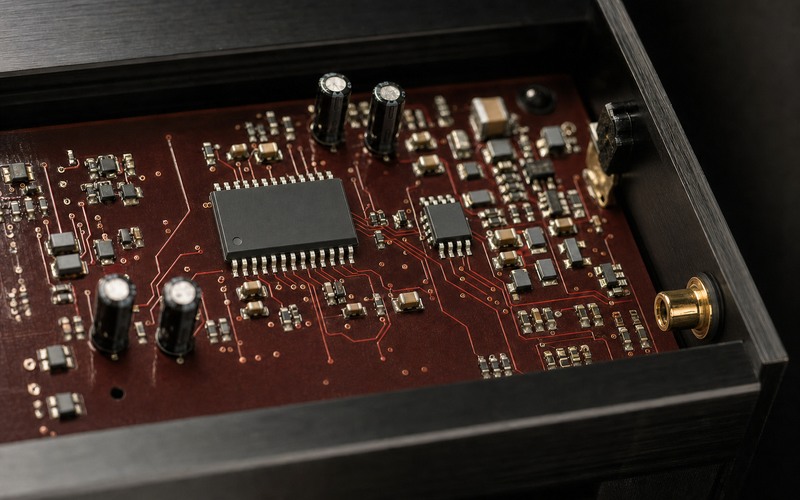
Confirm the exact PCM1702U identity
The base name PCM1702 describes the converter family, while the U suffix distinguishes the 20-pin SOIC form from the older 16-pin P package. Additional J or K grade markings identify tighter distortion selections in historical documentation. Packing and environmental suffixes can add more characters. Procurement, receiving and service records should preserve the full orderable code rather than shortening every device to PCM1702.
Package verification matters because the SOIC and DIP pin numbers are different even when signal names are shared. Build the symbol and footprint from the controlled drawing for the approved suffix. Record pin-one orientation, lead pitch, body width, solder fillet criteria and the exact assembly profile. A visually similar wide SOIC is not evidence of electrical interchangeability.
Treat the device as one audio channel
PCM1702 converts one channel. A stereo product uses two converters with separate current outputs and usually separate I/V paths. Channel matching then depends on converter grade, resistor ratios, op-amp offset and bandwidth, filter tolerances, rail noise and board symmetry. Two devices placed near each other do not create a matched stereo pair by themselves.
Keep left and right data ownership clear in the digital filter or serializer. Verify that the latch event for each converter occurs after its own 20-bit word is stable. During bring-up, drive one channel at a time and confirm connector identity, polarity, gain and idle offset before running stereo measurements.
Understand the segmented current-output architecture
The TI application note shows balanced current segments, an internal bipolar offset function, reference and servo circuits, and one IOUT node. Digital input activity steers internal current elements. The output is a current, so voltage is developed by the external I/V network. The architecture places supply and reference cleanliness directly inside the linearity and noise problem.
The specified bipolar output is around ±1.2 mA. Select the I/V feedback resistance from the desired output swing, then check op-amp headroom and the next stage. A larger resistance increases signal voltage but also changes noise gain, stability, resistor noise and overload margin. Use measured full-scale current and the approved analog target rather than copying a resistor from an unrelated DAC circuit.
Supply the four rail domains cleanly
Reference circuits show positive and negative analog rails and positive and negative digital rails, commonly tied to clean ±5 V sources at the system level while retaining local separation and bypassing. Confirm the controlled limits for the exact device before production. The negative analog rail deserves close attention because current segments connect into that domain and can couple rail noise into the output.
Place each local capacitor close to its associated pins with short connections to the intended return. Bulk capacitance belongs nearby but cannot replace high-frequency local bypassing. Keep regulator switching nodes, rectifier current loops and display or processor return currents away from the DAC reference and I/V area. Measure rail noise both at idle and while audio data is changing.
Define analog and digital ground paths
The device exposes analog and digital common connections. Ground planning should keep the DAC output and I/V feedback current in a compact analog loop while giving serial input current a direct return. Do not force the I/V loop to share a narrow trace with clock return current. A continuous reference plane with controlled current placement is often more predictable than a dramatic physical split.
If analog and digital ground regions meet at a planned location, verify that no connector shield, regulator or mounting point creates a second uncontrolled bridge. Review the complete enclosure and cable path. Audio hum and idle tones can enter through external grounding even when the local PCB looks orderly.
Match the serial data and latch timing
PCM1702 uses data, bit clock and latch-enable functions rather than a contemporary control bus with internal format registers. The source must deliver the expected 20-bit word, polarity and clock edge, then assert latch enable inside the specified setup and hold window. A stream that resembles I2S at first glance still needs a timing comparison at every relevant edge.
TI support describes the protocol as close to I2S, not identical to every I2S implementation. Check whether the source is left justified, how many clocks occur per word, where sign data appears and when the latch transfers the word into the DAC. Capture these signals at the receiver pins under process, voltage and temperature corners. Software labels for an audio port do not prove pin-level compatibility.
Choose the digital filter and sample path
The converter needs prepared serial sample data. Historical systems often paired it with an external digital filter that supplied oversampled words, bit clock and word latch timing. A new controller, FPGA or audio processor can perform that role if its framing is verified. Define source sample rate, interpolation, word length, truncation or dither, mute code and startup sequence as one signal-chain decision.
Do not infer that the DAC itself rejects out-of-band images. The external digital interpolation and analog reconstruction filter work together. Test passband response, stopband energy, intersample peaks and behavior at every supported sample rate. A design tuned around 44.1 kHz may require another filter response for 48 kHz material.
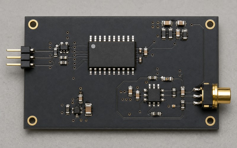
Design a stable current-to-voltage stage
The I/V amplifier holds the current-output node near its intended operating potential while converting DAC current into voltage. Select an op amp with adequate input behavior, noise, slew rate, gain-bandwidth and output swing on the available rails. The feedback resistor and capacitor set conversion gain and high-frequency stability. Input capacitance from the DAC, package and layout belongs in that stability analysis.
Keep the IOUT trace short and shield it from bit clock. Place the op amp and feedback components beside the converter so the summing node has little area. Use low-drift, low-excess-noise resistors with tolerance appropriate to channel matching. Verify settling on large code transitions and inspect the output for oscillation with the final cable and load connected.
Complete the analog reconstruction filter
The I/V output still contains spectral images and switching energy. A passive or active low-pass stage should meet the product bandwidth and attenuation target without consuming excessive phase margin or output headroom. Its source impedance, load and coupling method must be defined together with the next amplifier or connector.
Use audio measurements to check passband flatness, phase balance, noise, full-scale distortion and low-level linearity. Include several frequencies and amplitudes, not a single 1 kHz tone. The interaction between converter grade, I/V amplifier, feedback parts and reconstruction filter determines the finished channel.
Control clock coupling and idle tones
Bit-clock edges can couple through capacitance, shared impedance and power rails into the analog path. Keep clock routing short, avoid unnecessary edge-rate acceleration and do not run it alongside IOUT or the op-amp summing node. Series damping at the source may reduce ringing when supported by timing measurements.
Inspect the noise spectrum with zero code, low-level tones and changing sample data. Discrete spurs can reveal clock coupling, regulator interaction or periodic software activity that a broadband noise number hides. Repeat the test with nearby processors, displays and communication radios active in their demanding modes.
Plan startup, mute and power-down behavior
Bipolar rails, serializer activity and the downstream amplifier may become valid at different times. Define a sequence that holds the output path muted until the DAC data, latch timing, references, I/V stage and filter are stable. On shutdown, mute before the rails collapse. This prevents avoidable pops and protects high-gain downstream equipment.
Test cold start, warm restart, brownout, missing clock, repeated reset and one-rail failure. Check the current-output node and op-amp output during every transition. A relay or analog mute can be useful, but its contacts, timing and failure state need the same engineering review as the DAC circuit.
Measure grade and lot behavior
Historical J and K selections were associated with tighter distortion performance. Do not assume a generic U device meets a grade-marked requirement. Match the incoming full code to the approved bill of materials and retain traceability. Used, remarked or reclaimed parts create added risk for a discontinued precision converter.
Incoming evaluation can include marking and package inspection, X-ray or decapsulation through a qualified laboratory when risk warrants it, electrical identity checks and a controlled audio test. Compare offset, gain, noise, distortion and low-level behavior with known-good samples. A part that produces sound has not established precision performance.
Approach replacement as a redesign
TI states that no current catalog DAC is perfectly software compatible with PCM1702. A candidate such as a newer PCM-family device may accept a related audio stream, but it can require register programming, a new package, different supplies and another analog output stage. Mono and stereo options also change channel organization.
Build a comparison table for input framing, resolution, sample rates, control interface, output type, reference method, supply rails, package, lifecycle and measured performance. A voltage-output delta-sigma DAC may remove the classic I/V stage while adding its own filter and common-mode requirements. Treat firmware, schematic, layout and qualification as linked changes.
Prototype and verify the complete channel
Start with rail voltage, rail noise and serial timing at the device pins. Confirm correct full-scale polarity and output current, then bring up the I/V stage at conservative gain. Measure DC offset before connecting downstream equipment. Add the reconstruction filter and load only after each preceding stage behaves as expected.
Qualification should include frequency response, THD+N versus level and frequency, dynamic range, channel balance, crosstalk in stereo assemblies, idle spectrum, intersample overload, startup noise, temperature and supply tolerance. Keep the digital source, firmware revision, op amp, passive tolerances, load and instrument bandwidth with the results.
Finish the PCM1702U selection checklist
Before release, confirm the exact PCM1702U suffix, 20-pin SOIC footprint, discontinued status, authentic supply path, approved grade, 20-bit serial framing, latch timing, ±5 V rail plan, analog and digital returns, local bypassing, ±1.2 mA current-output assumption and I/V component values.
Review digital filtering, reconstruction filtering, clock routing, summing-node layout, channel matching, mute sequence, thermal behavior, incoming inspection and replacement strategy. A controlled design treats PCM1702U as one element in a complete precision audio path rather than as a line-level output component.
Related information
- 2026.07.17 LM35 as an Analog Voltage Temperature Sensor
- 2026.07.17 TMP102 for Low Cost Board Temperature
- 2026.07.17 TMP117 for High Accuracy Digital Temperature
- 2026.07.17 DS18B20 on a One Wire Temperature Bus


