 Free Shipping Over$200

- Products
- Marking
- Alternative

PI2PCIE2412ZHEX for PCIe Lane Switching
PI2PCIE2412ZHEX for PCIe Lane Switching
The PI2PCIE2412ZHEX belongs in a design only after the lane topology is drawn correctly. Diodes describes the PI2PCIE2412 as an eight-to-four differential-channel multiplexer and demultiplexer: four differential channels, equal to the transmit and receive pairs of two PCIe lanes, can be connected to one of two locations. It passes the physical signal in either direction. It does not enumerate endpoints, route transaction packets, create extra bandwidth or let two selected destinations operate at the same time.
The manufacturer rates the device for PCI Express 2.0 operation at 5.0 Gbps and lists a 1.5-to-1.8 V supply range with a ten-percent tolerance around the upper value. The current product page identifies a 42-contact ZH42 TQFN package, bit-to-bit skew up to 7 ps, channel-to-channel skew up to 35 ps, and crosstalk and off-isolation figures of -23 dB at 3 GHz. These figures describe the switch contribution. Board traces, connectors, vias, AC-coupling placement and the source and receiver still consume the rest of the link budget.
Diodes currently marks PI2PCIE2412 as not recommended for new design. That status changes the purchasing question. An existing qualified product may need controlled maintenance, exact-suffix procurement and a replacement plan. A new product should compare current alternatives before layout begins. The article keeps those two decisions separate and treats PI2PCIE2412ZHEX as an exact orderable record, not as a promise that every PI2PCIE2412 suffix has the same packing or qualification history.
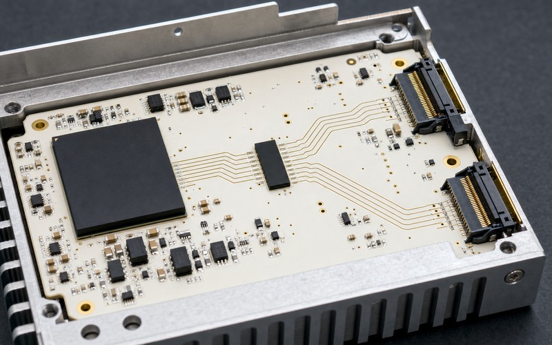
Draw the two-lane 2:1 topology first
A PCIe lane contains one transmit differential pair and one receive differential pair. Two lanes require four differential pairs, which matches the four differential channels in this part. In mux operation, the common four-channel side connects to either branch A or branch B under one select decision. In demux operation the electrical path is read in the opposite direction, but the same physical switch matrix is used.
This is different from a two-port PCIe packet switch. A packet switch terminates links, participates in protocol behavior and presents more than one downstream port to software. PI2PCIE2412 stays in the analog signal path. The root complex and endpoint still train directly across the selected route, and the unselected route is isolated rather than enumerated as another live device.
Use it where one host link must reach one of two mutually exclusive destinations: two alternate slots, a production connector versus a test connector, or a redundant module chosen before link training. If both endpoints must remain active, the architecture needs more lanes or a protocol-level PCIe switch.
Confirm that PCIe Gen2 is enough
The official rating is 5.0 Gbps PCIe 2.0 performance. A source and endpoint that negotiate Gen1 or Gen2 fit that signal-rate boundary. A Gen3, Gen4 or Gen5 link is outside the stated PCIe generation even if a short laboratory trace appears to train. Passing traffic on one board does not replace compliance evidence for the intended generation.
Bandwidth planning must also include lane width. This device handles two lanes, not four or eight. If a processor exposes an x4 link, routing only two lanes changes the available aggregate bandwidth and may alter how the endpoint is configured. Record the negotiated generation and width required by the application before the multiplexer is selected.
Treat it as a passive signal element
The device does not recover a clock or rebuild an eye. Every package pad, internal switch path and board discontinuity adds loss, reflection and skew to the end-to-end channel. Its low-skew figures help preserve pair alignment, but they do not cancel loss already created by long host traces, poor vias or a weak connector.
Diodes provides S-parameter and IBIS resources for the family. Use the applicable model in the channel simulation together with the processor package, board stack-up, via models, destination package and connectors. The result should be compared with the receiver requirements for the chosen PCIe mode.
If the route is too long for a passive switch, a redriver or retimer solves a different problem. A redriver reshapes the analog signal; a retimer recovers timing and transmits a new signal. Neither function is present inside PI2PCIE2412.
Do not hide this distinction in the bill of materials. The schematic symbol can look like a logic selector, yet the layout work is an RF channel design at multi-gigabit rates.
Place the narrow TQFN at the real branch point
The shortest practical arrangement places the 3.5 by 9 mm ZH42 TQFN where the common path divides. Long parallel stubs to the unselected destination can increase discontinuity even when that destination is isolated. Keep the host-to-switch and switch-to-connector segments intentional, and avoid routing a branch past its destination before turning back.
Preserve each differential pair
Route the positive and negative conductors of each pair together over one continuous reference plane. Use the impedance target and geometry derived from the fabricated stack-up, not a generic trace width copied from another board. Keep the pair away from plane splits, connector mounting holes and dense return-current obstacles.
Match the two conductors within a pair without adding large decorative serpentine sections. The switch data lists 7 ps maximum bit-to-bit skew, so excessive board mismatch can consume the advantage provided by the device. Match lane-to-lane timing only to the level required by the platform and layout rules.
Avoid test pads and probe stubs on production routes. For characterization, use a dedicated coupon or a fixture designed as part of the controlled channel. A small open stub can become a visible discontinuity at 5.0 Gbps.
Keep the return path through vias and connectors
A differential pair still drives return current through nearby reference structures. When the pair changes layers, place suitable ground return vias close to the signal vias. Do not send the pair across a void or from a ground-referenced layer to a power-referenced layer without a planned high-frequency return path.
The connector footprint belongs in the same analysis. Pad escapes, anti-pads, plated stubs and the connector launch can dominate a short route. Review both selectable destinations because their connectors or module footprints may differ.
Decide where AC coupling belongs
PCIe transmit paths use AC coupling, but the correct capacitor location follows the processor, endpoint and platform guidance. A bidirectional mux symbol can obscure which physical pair is the transmitter in each use case. Mark TX and RX direction for every selected route, then place capacitors once per required transmit path without creating duplicate series parts.
Capacitors should have a symmetrical footprint and a short, balanced escape. Their package and pad geometry become part of the differential channel. Do not place them merely to make the schematic look complete.
If a connector can accept different modules, confirm that the module does not add an unexpected second coupling set. The channel review should cover the assembled system, not the baseboard alone.
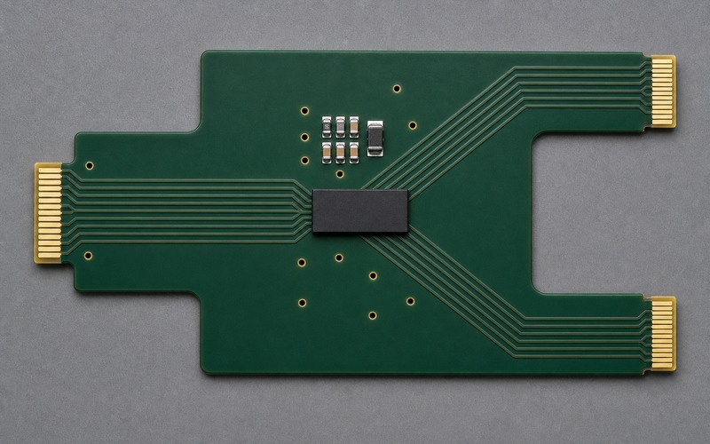
Power and control the 1.8 V device deliberately
The product page lists a supply range from 1.5 V to 1.8 V with tolerance around 1.8 V. Confirm that the local rail remains inside the controlled specification during power-up, steady operation and shutdown. Place decoupling close to the supply contacts and provide a low-inductance return.
The select and enable inputs are control signals, but their state decides which physical PCIe route exists. Hold them at a defined level before the root complex starts link training. Avoid a floating control during reset, and do not change selection while a live link is carrying traffic unless the complete platform sequence explicitly supports disconnect, retraining and power-state handling.
Plan the switching sequence with software
A safe sequence usually quiesces or removes the active endpoint, disables the link, changes the mux state, applies any endpoint-specific power sequence and then asks the root complex to discover the new path. The exact steps depend on the processor firmware, operating system and hot-plug capability.
The mux has no knowledge of that sequence. A control pin transition cannot make two endpoints exchange state cleanly by itself. Define ownership of reset, endpoint power, reference clock and presence detection alongside the select signal.
If selection is fixed at manufacturing time, use a stable strap and document the populated option. If it changes in service, include state feedback so software can determine which route was requested and whether the expected endpoint trained.
Read NRND as an engineering constraint
The current manufacturer page marks PI2PCIE2412 as not recommended for new design. It is not the same label as an immediate electrical failure, but it signals that a new platform should evaluate a current device family and long-term support path before committing a new footprint.
For an installed design, preserve the exact PI2PCIE2412ZHEX identity, approved manufacturer, ZH42 package, assembly profile and validated board revision. Check lifecycle notices and authorized supply documentation during each procurement review. Do not approve a related PI2PCIE part from its shared prefix alone.
Compare alternatives by more than pin count
A replacement review starts with topology, lane count, supported data rate, bidirectionality, control truth table, power rail, package dimensions and land pattern. Signal-integrity figures such as insertion loss, return loss, crosstalk, off isolation and intra-pair skew then decide whether the new part fits the same channel budget.
A newer PCIe generation rating can provide margin, but it may use another supply, pinout or package. A protocol packet switch is also not a drop-in replacement for a passive mux because it changes enumeration, clocking, power and software behavior.
Treat the substitute as a new high-speed channel until simulation and hardware measurements prove otherwise. Reuse of the same schematic net names does not prove electrical interchangeability.
Prototype with the worst selected path
Build and test both branches. The longer route, denser via field or weaker connector often sets the limit, but the shorter route can also suffer from a sharper launch or coupling discontinuity. Train every supported endpoint at the intended generation and lane width across power cycles and temperature conditions relevant to the product.
Measure margin instead of link-up alone
A link that reaches L0 once has not shown manufacturing margin. Use the platform's error counters, link retraining records and negotiated-speed logs during sustained traffic. Exercise resets, low-power states, endpoint changes and repeated cold starts.
For signal measurements, use the compliance method and fixtures appropriate to PCIe 2.0. Compare the selected route with a bypass or reference path where possible. Diodes' application material discusses using the PI2PCIE2412 with a signal conditioner when the channel extends beyond the passive path demonstrated in its example, which reinforces that route length belongs in the system decision.
Document the test board, stack-up, firmware, endpoint, connector and selected branch with the result. That record is needed when an alternate component or board revision is reviewed later.
Finish with a component and channel checklist
Confirm the exact PI2PCIE2412ZHEX order record, NRND status, 42-contact ZH42 TQFN, 1.8 V rail, four differential channels, two-lane 2:1 topology, Gen2 rate and select behavior. Confirm that only one destination is intended to be active.
Review stack-up, impedance, pair matching, reference planes, vias, AC coupling, connector launches, branch length, decoupling and control defaults. Verify both routes with the real root complex and endpoints, then retain simulation and measurement evidence with the approved material record.
Related information
- 2026.07.17 LM35 as an Analog Voltage Temperature Sensor
- 2026.07.17 TMP102 for Low Cost Board Temperature
- 2026.07.17 TMP117 for High Accuracy Digital Temperature
- 2026.07.17 DS18B20 on a One Wire Temperature Bus


