Free Shipping Over$200

- Products
- Marking
- Alternative

PCB vs PCBA: Key Differences Explained for Engineers and Buyers
PCB and PCBA are not the same. A PCB is a bare printed circuit board, while a PCBA is that board after components are installed, soldered, and tested. Understanding the difference helps prevent sourcing mistakes, cost surprises, and manufacturing delays.
Introduction: Why PCB vs PCBA Matters More Than You Think
In electronics development, the terms PCB and PCBA are often used interchangeably-especially by non-technical teams. However, for engineers, product managers, and sourcing professionals, misunderstanding the difference can lead to design delays, unexpected costs, and manufacturing risks.
Whether you are building a prototype, scaling into production, or outsourcing manufacturing, knowing what PCB and PCBA actually mean (and where responsibilities split) is a practical requirement-not just terminology.
What Is a PCB?
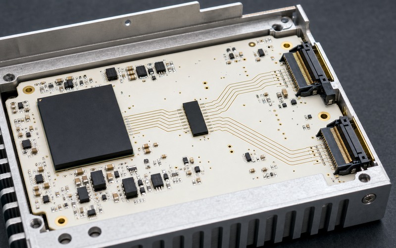
A PCB (Printed Circuit Board) is the bare board that forms the physical foundation of an electronic circuit. At this stage, there are no electronic components installed.
What a PCB Typically Includes
- Copper traces (routing) for electrical connections
- Insulating substrate (commonly FR-4)
- Vias, pads, and plated holes
- Solder mask and silkscreen
- Surface finish (e.g., ENIG, HASL, OSP)
What Is PCBA?
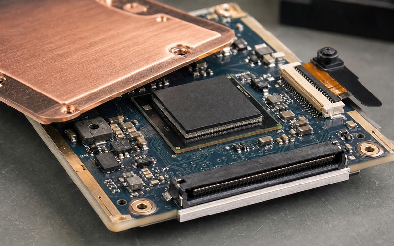
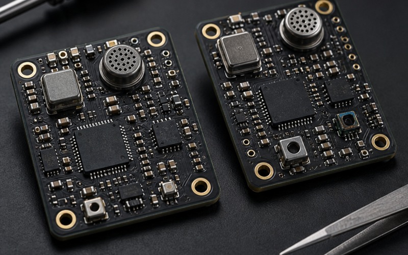
PCBA (Printed Circuit Board Assembly) refers to a PCB after components have been mounted and soldered. In other words, PCBA is the stage where a design becomes a working circuit module.
What a PCBA Typically Includes
- All passive and active components
- SMT and/or through-hole solder joints
- Inspection and testing (AOI, X-ray, functional tests as needed)
PCB vs PCBA: Core Differences at a Glance
| Aspect | PCB | PCBA |
|---|---|---|
| Component installation | No | Yes |
| Functional capability | Non-functional | Fully functional |
| Manufacturing scope | Board fabrication only | Fabrication + assembly |
| Required files | Gerber files | Gerber + BOM + Pick & Place + assembly notes |
| Cost structure | Materials + fabrication process | PCB + components + assembly labor + QA/testing |
| Typical testing | Electrical continuity / shorts | AOI, X-ray (if needed), functional tests |
Manufacturing Workflow Comparison
PCB Manufacturing Workflow (Bare Board)
- Design data preparation (Gerber export, drill files, stackup notes)
- Copper imaging and etching
- Layer lamination (for multilayer boards)
- Drilling and via plating
- Solder mask application and silkscreen printing
- Surface finish application
- Electrical testing and visual inspection
PCBA Assembly Workflow (Finished Board)
- Component sourcing (based on BOM and approved alternates)
- Solder paste printing
- SMT pick-and-place
- Reflow soldering
- Through-hole insertion (if required) and wave/hand soldering
- Inspection (AOI and/or X-ray depending on package types)
- Functional testing (as defined by the product requirement)
Cost Differences: Why PCBA Is More Than "PCB + Parts"
It's common for new buyers to assume that PCBA cost equals the PCB price plus component cost. In reality, PCBA pricing also reflects operational and quality requirements, such as:
- Procurement complexity and component availability risk
- Assembly setup (stencils, line programming, feeder setup)
- Machine time and skilled labor
- Inspection and testing requirements
- Yield management and potential rework
For low-volume production, setup and sourcing overhead can represent a significant part of the total, even when the PCB itself is inexpensive.
Design Responsibility: Where Problems Often Occur
A frequent misconception is that PCB design decisions do not affect assembly. In practice, a PCB can be electrically correct, yet expensive or risky to assemble due to manufacturing constraints.
Common Design-to-Assembly Pitfalls
- Footprints with incorrect pad dimensions (increases solder defects)
- Insufficient spacing (causes solder bridging or rework)
- Unclear polarity/orientation markings (increases assembly errors)
- Inconsistent reference designators (slows down verification and repair)
Designing with assembly in mind-often called DFM (Design for Manufacturability)-reduces defects, improves yield, and helps ensure the final board matches the original intent.
Typical Application Scenarios
When PCB-Only Orders Make Sense
- Early-stage R&D validation
- Education, lab experiments, and learning builds
- In-house component assembly or manual soldering workflows
When PCBA Is the Right Choice
- Commercial electronics products that require repeatability
- Industrial control boards and automation modules
- Automotive and medical assemblies where quality systems matter
- Pilot runs and mass production scaling
FAQ
Is PCBA always better than PCB?
Not necessarily. PCBA is required for a functional circuit board, but PCB-only orders are common for early-stage testing, education, or in-house assembly workflows.
Can I order PCB and PCBA separately?
Yes. You can fabricate PCBs first and outsource assembly later, but it typically increases coordination, risk, and lead time because multiple suppliers must align on revisions and quality expectations.
What files are required for PCBA?
Most assembly houses require Gerber files, a BOM (Bill of Materials), pick-and-place data (centroid file), and assembly drawings. Clear revision control and approved component alternates are also recommended.
Does PCB quality affect PCBA yield?
Yes. PCB fabrication quality directly impacts assembly yield and reliability. Issues like solder mask misalignment, inconsistent surface finish, or plating defects can cause soldering problems and rework.
Final Thoughts
Understanding the difference between PCB and PCBA is not just terminology-it affects cost, lead time, quality, and project success. A PCB is the foundation, while a PCBA is the finished, working assembly.
Treating PCB fabrication and PCBA assembly as distinct but tightly connected processes is a mindset shared by experienced engineers and professional electronics manufacturers-and it helps prevent many avoidable issues during development and production.