Free Shipping Over$200

- Products
- Marking
- Alternative

PCB Manufacturing Process: Step-by-Step Guide for Engineers
The quality of a printed circuit board is determined long before any components are assembled. Even the most advanced PCBA line cannot compensate for defects introduced during PCB manufacturing.
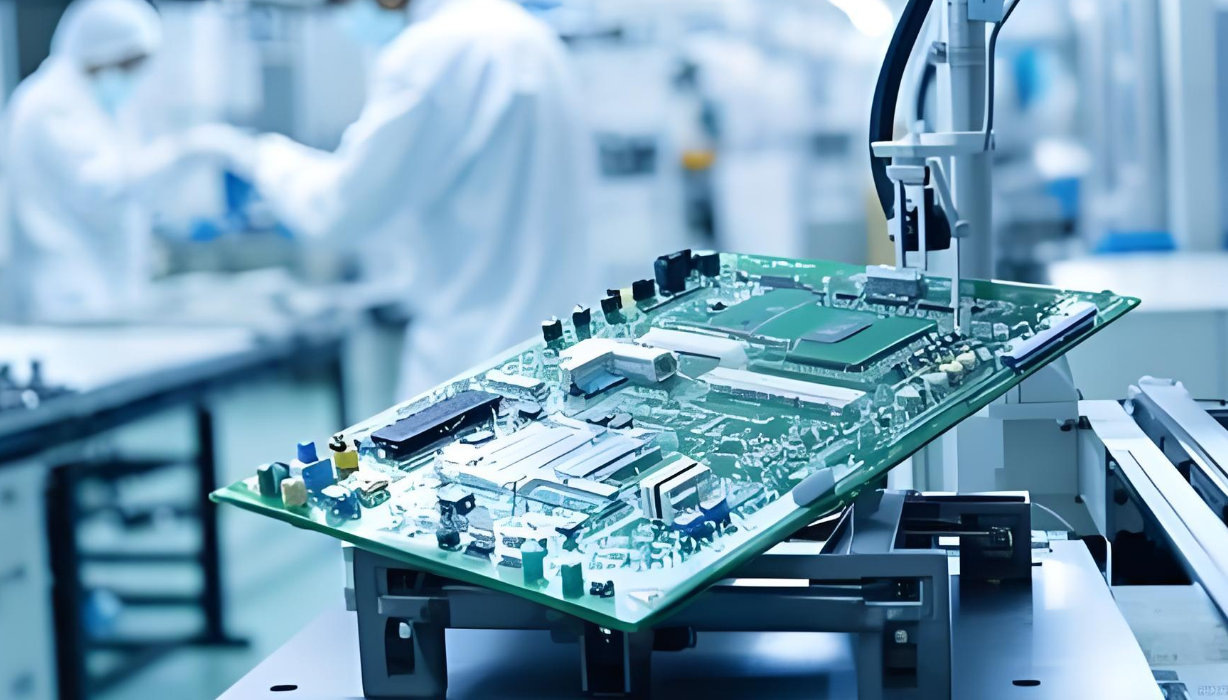
If you are not fully familiar with how a PCB is fabricated, it is easy to underestimate why certain design constraints exist or why specific manufacturing requirements are enforced. This guide walks through the PCB manufacturing process step by step, focusing on what matters most to engineers.
If you are still unclear about how PCB differs from PCBA, you may first read PCB vs PCBA: Key Differences Explained.
Overview: The Content Of PCB Manufacturing
PCB manufacturing refers to the fabrication of a bare printed circuit board, without any electronic components installed. The process converts design data into a physical board with copper traces, vias, solder mask, and surface finish.
Typical PCB manufacturing scope includes:
- Material preparation and layer stackup
- Copper pattern transfer and etching
- Drilling and via metallization
- Solder mask and silkscreen application
- Surface finishing and electrical testing
Step 1: Design Data Preparation
Everything begins with manufacturing data. PCB factories do not work directly from schematic files; they rely on standardized outputs.
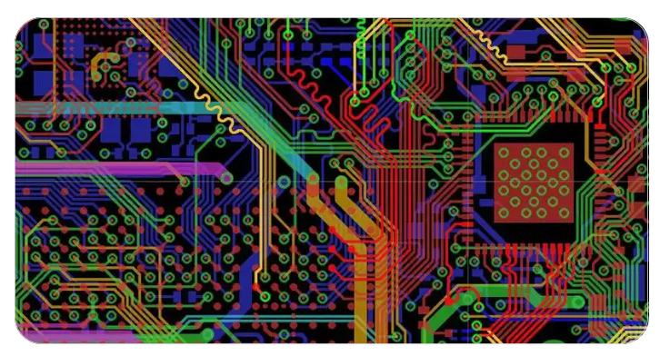
- Gerber files (copper, solder mask, silkscreen layers)
- NC drill files
- Stackup and impedance notes (for controlled designs)
- Fabrication drawings
Step 2: Inner Layer Imaging and Etching
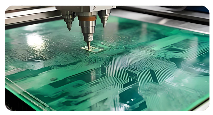
For multilayer PCBs, each internal copper layer is processed separately. A photoresist is applied, exposed, and developed to transfer the circuit pattern.
Unwanted copper is removed through chemical etching, leaving only the designed traces.
Step 3: Layer Lamination
Once inner layers are etched and inspected, they are stacked together with prepreg insulation and copper foil. The stack is then laminated under high heat and pressure.
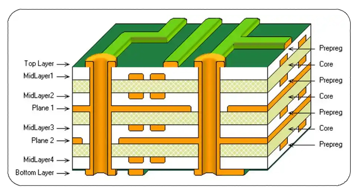
This step defines:
- Final board thickness
- Dielectric spacing
- Signal integrity characteristics
Step 4: Drilling and Via Metallization
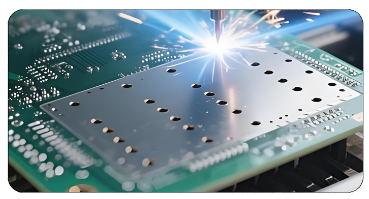
After lamination, holes are drilled for:
- Through-hole component leads
- Vias connecting copper layers
The drilled holes are chemically cleaned and plated with copper to create electrical connections between layers.
Step 5: Outer Layer Imaging and Plating
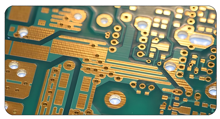
The outer layers follow a similar imaging process. Copper is plated to increase trace thickness, then etched to form the final outer-layer circuitry.
At this stage, the board has complete electrical connectivity.
Step 6: Solder Mask Application
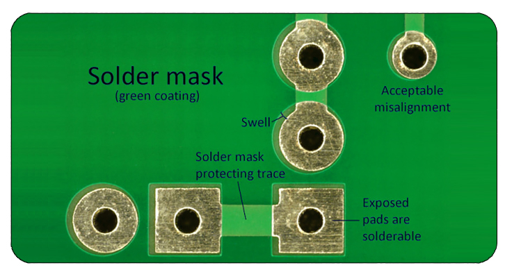
Solder mask is applied to protect copper traces and prevent solder bridging
during assembly.
Openings are defined only where components will be soldered.
Step 7: Silkscreen Printing
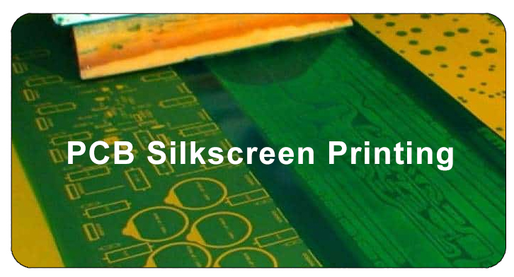
Reference designators, polarity markings, and logos are printed on the board surface. While often considered cosmetic, silkscreen clarity is critical for:
- Assembly orientation
- Debugging and repair
- Quality inspection
Step 8: Surface Finish
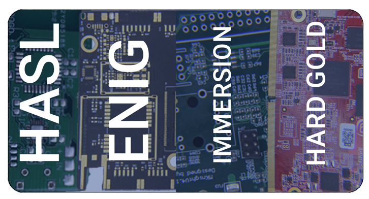
Surface finish protects exposed copper pads and ensures solderability.
Common options include:
| Surface Finish | Typical Use | Key Considerations |
|---|---|---|
| HASL | Low-cost, general electronics | Uneven surface, limited fine-pitch use |
| ENIG | Fine-pitch, BGA designs | Flat surface, higher cost |
| OSP | Cost-sensitive SMT boards | Limited shelf life |
Step 9: Electrical Testing
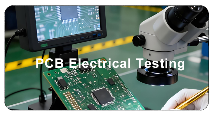
Before shipment, PCBs undergo electrical testing to verify:
- No shorts between nets
- All intended connections are present
This step ensures the board meets the electrical intent of the design, but it does not guarantee assembly success.
Common PCB Manufacturing Challenges
- Impedance mismatch due to stackup errors
- Annular ring violations
- Inconsistent copper thickness
- Solder mask misregistration
Most of these issues can be prevented by aligning PCB design decisions with fabrication capabilities early in the project.
How PCB Manufacturing Affects PCBA
PCB quality has a direct impact on assembly yield. Even a board that passes electrical testing can cause:
- Soldering defects
- Component misalignment
- Increased rework during PCBA
This is why PCB manufacturing and PCBA assembly should always be treated as interconnected processes.
Final Thoughts
PCB manufacturing is not a black box-it is a structured process where each step affects electrical performance, reliability, and cost.
Engineers who understand how PCBs are fabricated can design boards that are easier to manufacture, easier to assemble, and more reliable in the field.
In the next article, we will continue this workflow by explaining how a finished PCB becomes a functional product through PCBA assembly.