- Products
- Marking
- Alternative
XC17256EPCG20C as Configuration Memory for an FPGA Design
XC17256EPCG20C as Configuration Memory for an FPGA Design
XC17256EPCG20C looks like a small memory choice, yet it controls whether an FPGA wakes as the design that was approved. The device sits outside the logic fabric, holds the configuration bitstream, and has to deliver that data with the correct mode, voltage, clock relationship and reset behavior before any application code can prove the board works.
That makes this part a production risk item rather than a spare memory footprint. A board can have the right FPGA, the right power rails and a clean oscillator, then fail because the configuration memory suffix, package, programming path or reset polarity was copied from a nearby design without checking the real configuration chain.
Start with the Configuration Job
The job is narrow: store the bitstream that lets the FPGA become useful after power up. Older Xilinx serial configuration PROM families were built for this purpose, and the interface is much smaller than a general parallel memory bus. The FPGA and PROM exchange configuration data through a clocked serial path, with enable, data, reset and cascade behavior deciding whether the transfer starts and ends cleanly.
Keep the review tied to that job. Do not approve the part because its capacity number looks large enough in isolation. Confirm the actual bitstream size, configuration mode, FPGA family, programming tool, package, temperature grade and board access. If the selected memory is one-time programmable, the build process has to treat the loaded image as a release artifact, not as a field-update convenience.
The part also has to match the product life. A configuration memory chosen for an early lab board may be a poor production choice if the tool flow, programmer support, security policy or replacement route is weak.
Read the Suffix Before the Footprint
With configuration PROMs, the orderable string carries more meaning than the base family. Density, voltage family, package, temperature grade, lead finish and packing code can change the board fit or the purchasing result. XC17256EPCG20C should be checked as a full orderable part, not shortened casually to XC17256 during BOM review.
The footprint check should include pad style, body clearance, assembly orientation and programming access. A 20-lead package or socketed programming flow can impose a different inspection rule from a small serial flash package. If the approved footprint is built around a legacy PROM, a modern serial flash may not be a drop-in replacement even when both parts store an FPGA image.
Mark pin one and orientation in the assembly view. A configuration memory installed in the wrong rotation can leave the FPGA silent, and the fault may look like a power or clock problem until the board is inspected under magnification.
Confirm FPGA Mode and Clock Direction
The first electrical check is the FPGA configuration mode. In a master serial style connection, the FPGA supplies the configuration clock and reads data from the PROM. In a slave serial style connection, the clock comes from an external source. The chosen mode changes which signal owns timing and which side must be stable first.
The board record should name the clock source, configuration pins, pull states and reset path. It should also state what happens after configuration completes. Some designs disable the PROM after loading. Others keep access for diagnostics or reconfiguration. The schematic should make that state visible rather than relying on tribal memory.
Clock and data traces are short on many boards, but they still deserve a route review. Keep the clock away from a noisy switching node, avoid long loops through the board, and keep the return path clean. A configuration fault at cold start can be rare enough to escape a quick bench test and frequent enough to create field returns.
Capacity Is a Bitstream Question
Do not treat the memory density as a marketing number. Compare it with the actual FPGA bitstream generated by the selected tool settings. Compression, startup options, unused logic, debug cores and revision choices can change the file. A design that fits in the lab image may exceed the selected PROM after a late logic block, debug feature or security option is added.
Keep a margin policy in the design record. The point is not to chase a huge memory by habit. The point is to leave enough room for the approved bitstream path while avoiding a part that is harder to buy, program or second source. For a legacy OTP PROM, every image change has a cost in scrap, labels, records and requalification.
Capacity review also covers cascaded devices. If one PROM cannot hold the image, the chain must be reviewed as a system: device order, CEO behavior, clock loading, board route, programmer support and test coverage.
Programming Flow Belongs in the BOM Review
A configuration memory is not approved until the team can program and verify it using a controlled process. That process may happen before placement, through a socketed programmer, or after assembly through board access. Each route changes purchasing, incoming inspection and production test.
For XC17256EPCG20C style parts, the buyer should not accept a vague promise that the PROM is programmed. The release package needs the bitstream file, checksum or identification method, programmer setup, label rule, handling rule and retest method. Without those details, two boards with the same printed BOM can contain different logic images.
Production should also know how failures are separated. A blank PROM, wrong image, wrong polarity, damaged package and solder fault can all produce a dead FPGA at first power. A test plan that checks supply current, configuration pins, clock movement and DONE or equivalent status makes repair practical.
Reset and Power Order Decide First Boot
The FPGA, PROM, oscillator and power rails do not become valid at the same instant. The reset network must hold the configuration path in a known state until supplies and clock are ready. If reset releases too early, the FPGA may sample a weak data line or start a transfer while the memory is still settling.
Check both rising and falling cases. Power cycling, brownout, sleep recovery and manual reset can exercise different timing edges. A board that configures after a slow bench supply ramp may fail when the final product uses a fast regulator or when a battery droops during radio transmit.
Pull resistors matter. The mode pins, enable pins and reset pins should not float during power transition or programming. The approval record should state the intended default state and the resistor values used to create it.
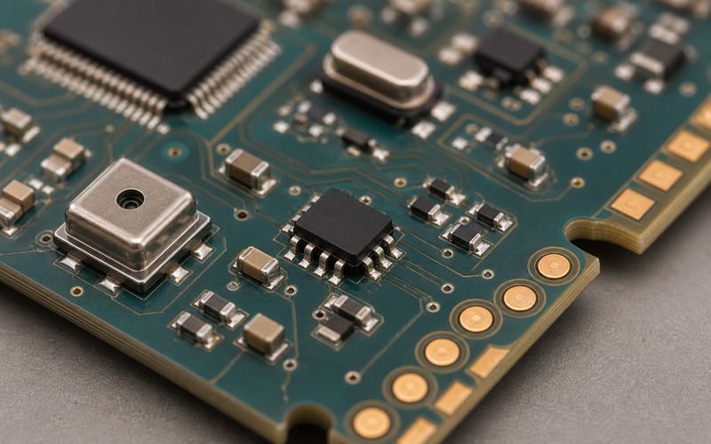
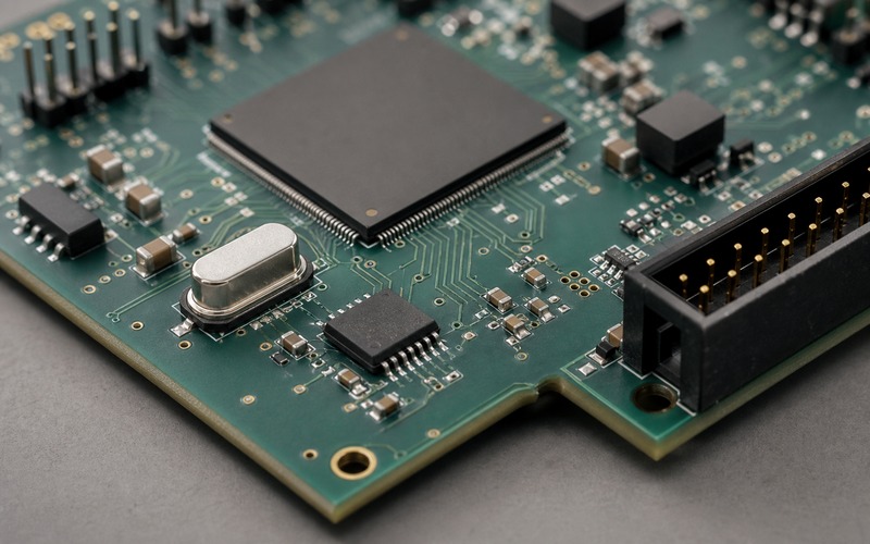
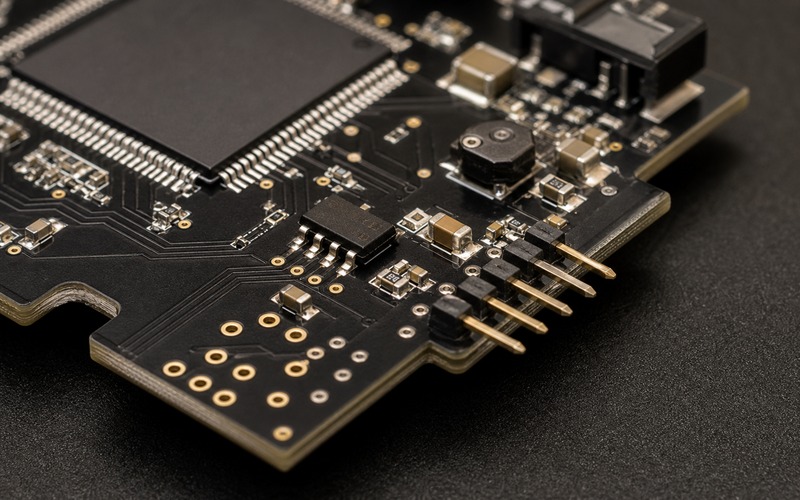
Layout Should Show a Service Path
The physical placement needs to make the configuration chain readable. Put the PROM close enough to the FPGA for a clean serial route, but leave access for inspection and programming. The programming header should face a board edge or a known fixture access direction. A hidden header under a cable, shield or heat spreader slows every failure analysis case.
Decoupling should sit near the PROM supply pins, and the route from PROM to FPGA should avoid crossing the highest current power path. If a board needs an in-circuit programmer, the connector orientation must allow a cable or pogo fixture to reach it without pressing against a fragile component.
The inline image follows this check: configuration memory, reset path, programming pins and board edge access are visible as one service area rather than scattered details.
Substitution Needs More Than Memory Size
A replacement part must match more than capacity. Review programming method, OTP or reprogrammable behavior, voltage levels, package, pinout, reset polarity, cascade support, clock relationship, tool support, programmer support, lifecycle status and available test evidence. A common serial flash can be the right substitute in a redesigned boot chain, but it is not automatically a substitute for a dedicated legacy serial PROM footprint.
Second sourcing should be written as a controlled engineering option. If the alternate requires a new footprint, a different FPGA mode, a different programmer or a revised production test, it belongs in a new board spin or a qualified variant, not as a purchasing swap.
Buyers also need to watch suffix drift. A near name can differ in temperature range, package style or lead finish. The purchasing record should keep the full approved part string and the exact image or programming status expected on delivery.
Inspection and Failure Checks
Incoming inspection can verify label, package, moisture handling, programming status if available, and evidence that the supplier understood the full orderable part. After assembly, test should prove that supplies are present, reset releases as intended, configuration clock moves, data is available, and the FPGA reaches the configured state.
Keep a short dead-board checklist. Check PROM orientation, solder joints, supply rail, reset pin, clock pin, data line, enable line, programming header continuity and FPGA mode pins before replacing the FPGA. Many configuration failures are cheaper to find around the small memory than around the large programmable device.
If the bitstream is protected or cannot be read back, the process still needs a verification method. Checksum records, programmed-lot records, fixture logs and a known functional test become part of the component approval evidence.
Board Revision Control
The configuration memory also ties the board revision to the logic revision. A layout change that moves a mode pin, changes the oscillator, swaps a regulator, changes pull resistors or moves the programming connector can require a new boot check even when the FPGA and PROM part numbers stay the same. Keep the approved image, schematic revision and board revision in the same release record.
Prototype labels should separate blank devices, programmed devices and devices loaded with an engineering image. Mixing those states creates a failure that looks random because the assembly can be electrically sound while the logic image is wrong. A small label rule and a fixture log prevent many hours of board debug.
When a later production lot uses a substitute programmer, a different fixture cable or a new programming house, repeat the first boot test on real boards. The test should prove configuration timing, DONE or equivalent status, basic I/O behavior and current state after loading. That evidence is stronger than a purchase note saying the memory was programmed.
Final XC17256EPCG20C Selection Checklist
Before approving XC17256EPCG20C, confirm bitstream size, FPGA configuration mode, full suffix, voltage family, package, programming flow, reset polarity, clock source, cascade behavior, board edge service access, decoupling placement, production test and approved alternates. Do not add body links unless the target page has been checked live and returns a stable page.
The part is a good choice when it makes the FPGA boot path predictable and inspectable. It is a risky choice when the team treats it as a generic memory chip and leaves programming, reset, suffix and test evidence for production to discover later.