- Products
- Marking
- Alternative
CrossLink-NX Handling Parallel Image Sensor Data
CrossLink-NX Handling Parallel Image Sensor Data
CrossLink-NX earns attention when an image sensor still speaks in a parallel format but the rest of the product has moved toward compact processors, serial links and stricter power budgets. The part is useful as a bridge and timing guard: it can sit close to the camera connector, capture pixel lanes, align frame signals and present a cleaner stream or event boundary to the host.
The selection question is not whether an FPGA can move image data. It is whether this device can own the sensor-facing timing without turning into a full video processor. A good design keeps the fabric close to the connector, gives each signal a clear bank and clock domain, and leaves enough debug visibility to prove that dropped pixels are electrical or timing faults rather than image content.
Start with the Sensor Bus
A parallel image sensor interface is more than a bundle of data pins. It carries pixel clock, horizontal timing, vertical timing, reset, standby, control bus lines and power sequencing assumptions. The part review should name each signal and state which edge or level matters. If the team only counts data width, the board can still fail at frame start, first line timing or sleep recovery.
CrossLink-NX fits when the sensor bus needs a compact programmable boundary. The FPGA can absorb pin mapping, line timing, polarity changes, simple packing and a format handoff. That boundary is useful when the host package does not expose the right camera pins, when the host needs a calmer interface, or when the board may change sensors during early product work.
The decision should stay narrow. If the design needs demosaic work, image correction, large buffering or model inference, those jobs belong elsewhere. This stage should protect timing and reduce interface risk.
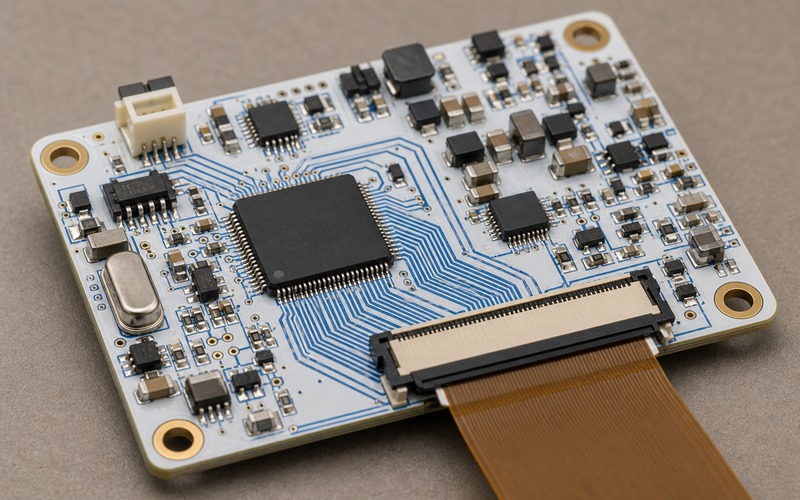
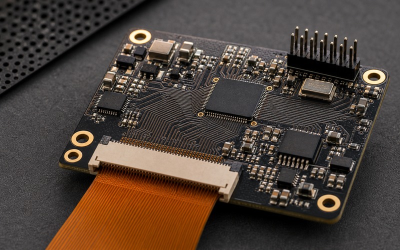
Place the FPC Connector at the Board Edge
The camera FPC connector is a mechanical and electrical part of the selection. It should face the edge where the cable can enter without folding across the FPGA, oscillator, regulator or debug header. A connector that opens toward the center of the board may look tidy in a render, but it creates a cable path that fights assembly and makes the signal path harder to inspect.
Keep the data fanout short and readable. The board should show a direct path from FPC pins into the FPGA bank, with reference ground nearby and no avoidable detours through a regulator area. If the sensor connector must sit at an angle because of the enclosure, record that condition before the pin map is approved.
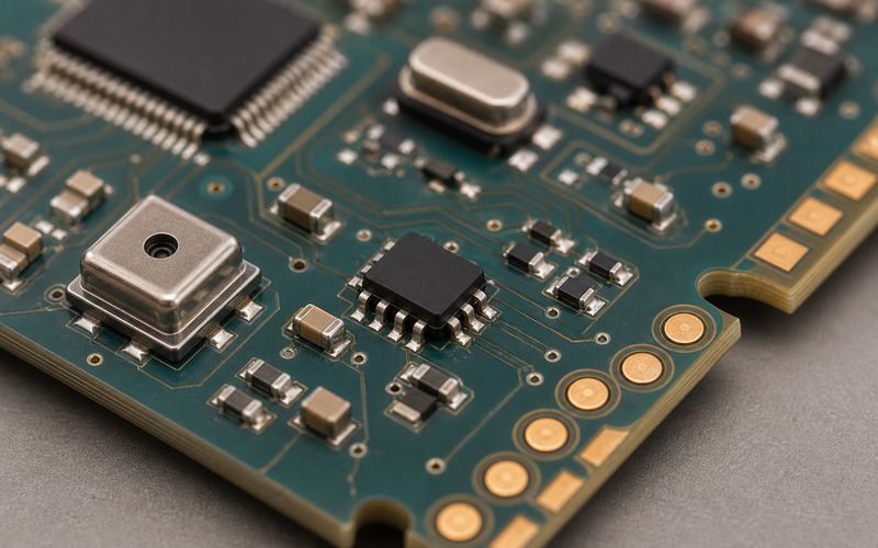
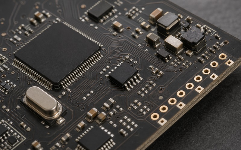
The local images use two board styles for this reason: the cover shows the whole bridge area for list-card recognition, while the inline image tightens around the FPC connector, fanout, FPGA pins and clock area.
Check I/O Banks Before the Package Looks Approved
The first package question is not size. It is whether the chosen I/O banks can support the sensor voltage, pin count, clock input and host-facing interface at the same time. A package that looks pin-rich can still block the route if the needed pins sit in the wrong bank or force clock and data across awkward sides of the chip.
Bank voltage, input threshold, output drive, pull state and reset state should be written beside the signal list. A camera sensor may use one rail for I/O and another rail for analog or core power. The bridge has to respect those rails without leaving translators awake during low power states.
Pin assignment deserves an early layout pass. Assigning all data pins in numeric order may make firmware tables simple, but it may twist the fanout from the FPC. A route-friendly pin map can save board layers and make timing closure less fragile.
Clock Domains Need a Written Boundary
Parallel image data is clocked data. The design should state whether CrossLink-NX receives the sensor pixel clock, generates a related clock, crosses into another domain or forwards timing to a host. Each choice changes constraints, reset behavior and debug checks.
Clock startup should be tested as a repeated state transition. Power the sensor rail, release reset, start the clock, configure the FPGA and capture the first valid line many times. A first-frame error after sleep can disappear during continuous streaming, so a single long capture test is weak evidence.
Give the design a few status counters. Frame count, line count, short line, long line, missing sync, pixel overflow and clock-loss flags make bring-up practical. They also help separate board timing problems from optical changes during later camera tuning.
Configuration Memory Is Part of the Interface
The FPGA image, configuration flash, reset circuit and programming access belong in the same review as the sensor bus. A bridge that cannot be recovered after assembly is a risk, even if the pixel path works in the lab. Keep programming pads, debug pins or a service connector reachable after the camera bracket, shield or enclosure is installed.
Configuration time should be placed in the camera wake sequence. If the host expects a frame too soon, a correct bridge can look broken. The approval record should include boot mode, configuration source, reset order, first valid frame timing and the bitstream version used for validation.
Changing the sensor later may require a new FPGA image. That update path needs version control and a rollback plan. If the bitstream is fixed for product life, record the exact sensor mode, data width, pixel clock and output format that were validated.
Decide the Host Interface Early
The host side can be a parallel bus, a narrow control interface, a serialized stream, a memory-like interface or an event signal, depending on the product. CrossLink-NX should reduce mismatch, not hide a vague system boundary. Decide what the host receives before the PCB route starts.
If the host receives every pixel, the FPGA acts as a timing and pin bridge. If the host receives a cropped window or compact event, the FPGA is doing preprocessing and needs deeper test coverage. If the host receives only a wake signal, the product must prove that missed events are rare enough for the use case and that the camera state is repeatable.
Keep the host interface testable. A fixture should be able to feed a known pattern or sensor emulator and check that the host boundary receives the expected timing, count or packet.
Power Sequencing Controls Reliability
Camera modules often have several rails and a strict reset rhythm. The bridge stage should not assume the sensor is ready because the digital I/O rail is present. Analog rail, core rail, clock, reset and standby each influence the first valid output.
Sequence evidence should include current state and signal state. Record sensor off, FPGA configured, clock present, reset released, first valid line, host handoff and return to low power. That evidence helps find a regulator that wakes slowly, a pull-up that leaks current or a clock source that starts outside the expected window.
Low current states need their own checks. A line held high through a pull-up, a translator left enabled or a clock source left running can erase the power reason for adding a small bridge device.
Signal Integrity Is Still a Board-Level Job
Parallel image buses can look forgiving because the traces are short. Short does not mean careless. A tight FPC pitch, fast edge rate, shared return path, nearby regulator or poor connector footprint can still create intermittent errors. Keep data, clock and sync groups close enough to inspect and separated enough from noisy power parts.
Length matching should follow the actual sensor timing need rather than a decorative routing rule. Some buses tolerate modest mismatch, while others need more discipline around clock-to-data arrival. The design record should state the target and the reason, so layout review and future board spins do not rely on memory.
Put the oscillator and configuration memory where they do not force the pixel fanout into a long detour. The inline image direction makes this visible: connector, trace fanout, FPGA pins and timing parts should read as one engineering area.
Substitution Review
An alternate bridge device has to match package, I/O bank structure, configuration method, tool flow, memory resources, clocking options, current profile and lifecycle status. Logic capacity alone is a weak comparison. A similar device can still fail because the bank layout changes the FPC escape or because the configuration sequence no longer fits the camera wake path.
Supporting parts also need alternates. A configuration flash, oscillator, regulator, FPC connector or ESD part can block production if it is approved casually. Keep each supporting part tied to the signal or power condition it protects.
For purchasing review, record the exact package, temperature range, sensor mode, bank voltage, connector orientation, configuration memory and approved output boundary. That record lets a buyer ask for an equivalent without accidentally changing the camera interface.
Bring-Up Checks
Bring-up should begin with power rails, configuration, oscillator, reset and a static pattern. Then move to line timing, frame timing, host handoff and low power recovery. This order isolates faults. Starting with a live camera scene makes optical noise, sensor setup and board timing compete for attention.
A small test pattern can catch many faults. Check bit order, polarity, frame start, line length, dropped pixel count and host event output. Repeat the same test after cold start, sleep recovery and sensor reset.
Keep the results with the board revision. The useful record names bitstream version, sensor mode, power state, clock setting and measured failure boundary.
Production Limits Need Plain Evidence
Production review should avoid a vague pass mark such as camera works. A practical fixture can check configuration, pixel clock presence, sync polarity, line count, short packet output and current in a few states. The fixture does not need a beautiful image. It needs a repeatable signal that proves the connector, FPGA bank, clock path and host boundary still match the approved design.
Keep limits tied to the board and sensor mode. A later camera change, FPC supplier change, oscillator change or package change can then be judged against the same evidence. This makes the bridge stage easier to buy, inspect and repair without turning every substitution request into a full system redesign.
Final CrossLink-NX Selection Checklist
Before approving CrossLink-NX, confirm sensor bus width, FPC orientation, I/O bank voltage, clock domain, configuration path, host boundary, power sequence, debug counters, test access and substitution limits. Do not add body links until the target page is confirmed live.
The part is a good fit when it keeps parallel sensor timing close to the camera and gives the host a cleaner boundary. It is the wrong place for broad image processing, large frame storage or work that changes with every model build.