 Free Shipping Over$200

- Products
- Marking
- Alternative

Analog Devices Inc./Maxim Integrated MAX662ACSA+T
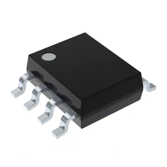
- Part No.:
- MAX662ACSA+T
- Manufacturer:
- Analog Devices Inc./Maxim Integrated
- Package:
- 8-SOIC (0.154", 3.90mm Width)
- Datasheet:
-
 MAX662ACSA+T.pdf
- Description:
- IC REG CHARG PUMP 12V 30MA 8SOIC
- Quantity:
Unit Price:$0.000000
Ext Price:$0.000000
- Payment:

- Shipping:

Inventory:2,809
Send us your inquiry,we will respond immediately.
In Stock : 2,809 PCS
| Qty. | Unit Price | Ext Price |
| 0+ | $0.000000 | $0.000000 |
*Products eligible for online ordering ship within 1-2 business days,please contact us for exact shipping times.
Also you can RFQ for MAX662ACSA+T or email to us: Email: [email protected] , we will contact you within 12 hours.
Product Details
MAX662ACSA+T - Maxim MAX662A +12 V, 30 mA Charge-Pump (Flash Memory Programming Supply), Inductorless, 8-Pin SO | MAX662A
MAX662ACSA+T is the lead-free, tape-and-reel 8-pin SO version of Maxim's MAX662A, a regulated +12 V, 30 mA charge-pump DC-DC converter made for generating the flash-memory programming voltage (VPP) from a logic supply. It needs no inductor - only four small capacitors - delivers a regulated +12 V ±5% guaranteed at 30 mA from a 4.5 V to 5.5 V input, draws just 185 µA quiescent, and has a logic-controlled 0.5 µA shutdown. Fitting in about 0.1 in² of board, it suits flash-memory programming, compact +12 V op-amp supplies, switching low-voltage MOSFETs and dual-output +12 V/+20 V supplies.
Product Introduction
The MAX662A from Maxim Integrated (now part of Analog Devices) solves a specific board-level problem: a 5 V digital system that must also produce the +12 V a flash memory needs for programming and erase. Rather than add an inductor-based boost regulator, the MAX662A uses a charge pump - a switched-capacitor converter that needs no inductor, only four capacitors - so it generates the +12 V quietly and in minimal space. It is an upgrade of the original MAX662, and MAX662ACSA+T is the RoHS ("+"), tape-and-reel ("T") 8-pin SO option.
The output is regulated, not just multiplied: +12 V ±5% is held while the converter sources a guaranteed 30 mA - enough to program the flash device. The input is a standard logic rail, 4.5 V to 5.5 V, and the quiescent current is a low 185 µA. When the +12 V is not needed, a logic-controlled shutdown (SHDN̅) drops the supply current to 0.5 µA and the output is disconnected - important in a battery or standby system where the programming voltage is only needed occasionally.
The switched-capacitor topology is built around two flying capacitors on the C1+/C1- and C2+/C2- pins, plus input and output reservoir capacitors - the "four capacitors, no inductor" that keep the solution small (about 0.1 in²) and free of the EMI an inductor can radiate. The MAX662A handles the regulation internally, so the designer only sizes the capacitors per the datasheet. It operates over the commercial 0 °C to +70 °C range (C grade) in the 8-pin SO.
Expert Technical Insight
How is the charge pump applied, and what should the designer check?
- Pick the four capacitors per the datasheet: two flying caps (C1, C2) and the input/output reservoirs set the converter's behavior. Use the recommended values and low-ESR types so the +12 V holds ±5% at the full 30 mA - undersized caps drop the output under load.
- Use SHDN̅ for occasional VPP: flash programming is intermittent, so gate the +12 V with the logic shutdown - 0.5 µA when off versus 185 µA running. The output disconnects in shutdown, so nothing back-feeds the flash VPP pin when programming is idle.
- Mind the 30 mA budget and the input range: the guaranteed output is 30 mA at +12 V from 4.5-5.5 V; keep the load within that, and bypass the 5 V input well since the charge pump draws pulsed current. The inductorless design avoids EMI, but the switching frequency still warrants a clean layout around the flying caps.
Key Benefits
A regulated +12 V ±5% output guaranteed at 30 mA - the flash-memory programming voltage from a 5 V rail.
A switched-capacitor charge pump needs no inductor, only four capacitors, fitting ~0.1 in² with no inductor EMI.
Low 185 µA quiescent current, with a logic-controlled 0.5 µA shutdown for intermittent VPP.
Runs from a standard 4.5 V to 5.5 V logic rail in a compact 8-pin SO (or DIP) package.
Specifications
| Parameter | Value | Condition / Note |
|---|---|---|
| Device Type | Regulated Charge-Pump DC-DC | Flash VPP supply |
| Manufacturer | Maxim Integrated (Analog Devices) | MAX662A |
| Output Voltage | +12 V ±5% | Regulated |
| Output Current | 30 mA | Guaranteed |
| Input Voltage | 4.5 V to 5.5 V | Logic rail |
| Topology | Switched-capacitor (inductorless) | Only 4 capacitors |
| Quiescent Current | 185 µA | |
| Shutdown Current | 0.5 µA | Logic-controlled (SHDN̅) |
| Board Area | ~0.1 in² | Compact |
| External Components | 4 capacitors | No inductor |
| Operating Temperature | 0 to +70 °C | C grade (commercial) |
| Package | 8-Pin SO | Outline 21-0041 (narrow SO) |
| Orderable Part Number | MAX662ACSA+T | Pb-free, tape and reel |
Note: Values are taken from the Maxim MAX662A datasheet. Confirm every parameter and the recommended capacitor values against the latest official documentation before committing a design.
Package Information
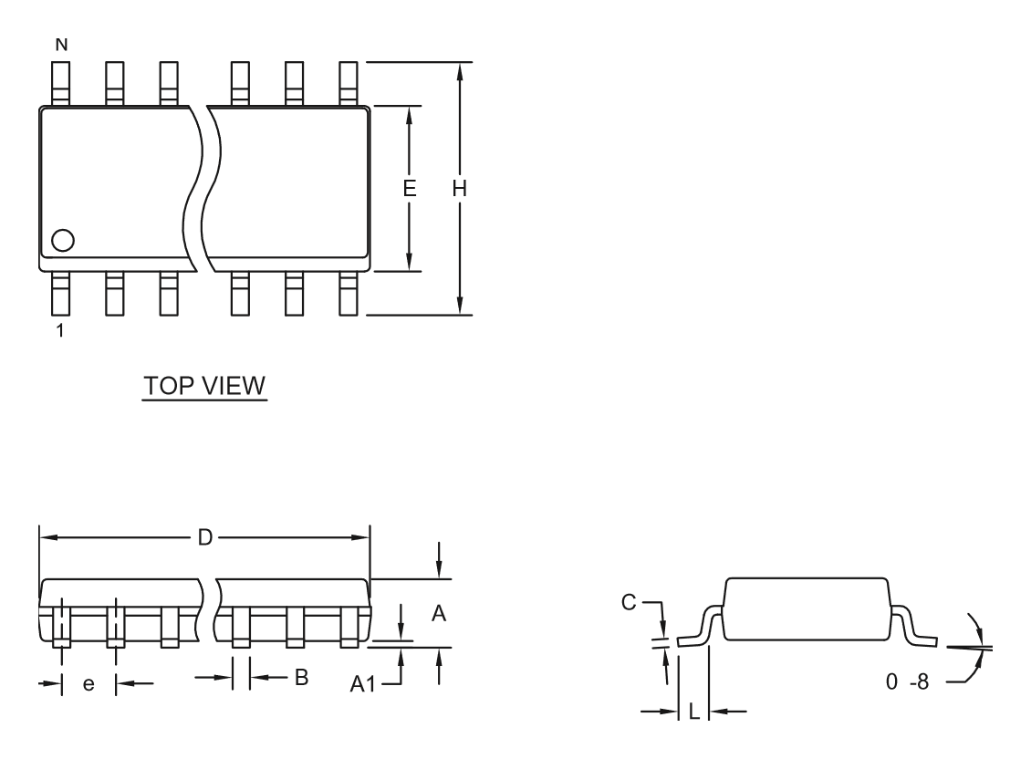
MAX662ACSA+T ships in the 8-pin SO (0.150-inch narrow SOIC, package outline 21-0041) - the small body that, with only four external capacitors, lets the whole +12 V generator fit about 0.1 in². Place the flying capacitors (C1, C2) close to the C1+/C1-/C2+/C2- pins, keep the reservoir caps at IN and OUT, and route the switched nodes short to contain the pulsed currents. The dimensional drawing below gives the full mechanical detail.
Pin and Signal Definition
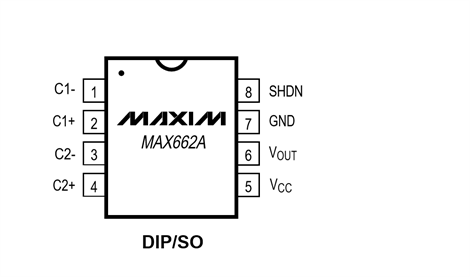
The 8-pin SO carries the two flying-capacitor pairs, supply, output and shutdown (per the MAX662A datasheet):
- Pin 1 - C1-: Flying capacitor 1, negative terminal.
- Pin 2 - C1+: Flying capacitor 1, positive terminal.
- Pin 3 - C2-: Flying capacitor 2, negative terminal.
- Pin 4 - C2+: Flying capacitor 2, positive terminal.
- Pin 5 - VCC: Supply input, 4.5 V to 5.5 V; bypass to GND.
- Pin 6 - VOUT: Regulated +12 V output; reservoir capacitor to GND.
- Pin 7 - GND: Ground.
- Pin 8 - SHDN̅: Logic shutdown input (active-low); 0.5 µA standby, output disconnected.
Alternative and Related Parts
The MAX662A is a dedicated +12 V flash-VPP charge pump. The related parts below are other power-management and supervisory devices that share a system with it.
| Part Number | Brand | Type / Relation | Package | Note |
|---|---|---|---|---|
| MAX604CSA+T | Maxim | 3.3 V LDO regulator | 8-SO | Logic-rail supply |
| MAX6368LKA29+T | Maxim | µP supervisor, battery backup | 8-SOT23 | Memory protection |
| MAX6369KA+T | Maxim | Watchdog timer | 8-SOT23 | µP supervision |
| MAX5921EESA+ | Maxim | -48 V hot-swap controller | 8-SO | Power-path control |
| MAX5980GTJ+T | Maxim | Quad PoE PSE controller | TQFN | Power delivery |
Selection Tips: Choose the MAX662A when a 5 V system needs a small, inductorless, regulated +12 V at up to 30 mA - typically a flash-memory VPP rail. Pair it with an LDO (MAX604) for the logic rail and a supervisor/watchdog (MAX6368/MAX6369) for the processor housekeeping around the flash device.
Manufacturer Information
Maxim Integrated, now part of Analog Devices, Inc. (ADI), built the MAX662A to give a 5 V board a small, quiet +12 V supply for flash programming - a regulated charge pump that needs no inductor and only four capacitors, with a logic shutdown for intermittent use.
ADI maintains the datasheet, the capacitor-selection guidance and the load/regulation specifications for the part - the basis for a dependable +12 V VPP rail in minimal board area.
Applications

Frequently Asked Questions
What is the MAX662ACSA+T output?
A regulated +12 V ±5%, guaranteed at 30 mA, generated from a 4.5 V to 5.5 V logic rail. It is a charge-pump (switched-capacitor) DC-DC converter intended as a flash-memory programming voltage (VPP) supply.
Does it need an inductor?
No. The MAX662A is a charge pump and uses only four capacitors - two flying capacitors (C1, C2) plus input and output reservoirs - so the whole +12 V supply fits about 0.1 in² with none of the EMI an inductor can radiate.
How much current does it draw?
185 µA quiescent while running, and just 0.5 µA in the logic-controlled shutdown (SHDN̅). Because flash programming is intermittent, gating the +12 V with shutdown keeps the average current very low.
What package and temperature range?
An 8-pin SO (narrow SOIC, outline 21-0041), rated 0 °C to +70 °C (C grade). With only four external capacitors the solution is compact - about 0.1 in² - and easy to lay out beside the flash device.
Disclaimer
Information Accuracy: The specifications on this page are based on the official Maxim MAX662A datasheet. We work to keep the information accurate and complete, but parameters can change with product revisions, so design engineers should verify all values against the latest official documentation before final design.
Product Authenticity Guarantee: All parts we supply are genuine factory originals with full material traceability.
Technical Support: Pre-sales and post-sales technical consultation is available free of charge.
Application Notice: This page is for reference only. Suitability for a specific application should be confirmed by the design engineer against the actual system requirements.
MAX662ACSA+T Specifications
- Specifications
- Attributes
- Property Value
- Manufacturer
- Analog Devices Inc./Maxim Integrated
- Series:
- -
- Package/Case:
- 8-SOIC (0.154", 3.90mm Width)
- Packaging:
- Tape & Reel (TR)
- Part Status:
- Active
- Function:
- Step-Up
- Output Configuration:
- Positive
- Output Type:
- Fixed
- Number of Outputs:
- 1
- Voltage - Input (Min):
- 4.5V
- Mounting Style:
- Surface Mount
- Voltage - Input (Max):
- 5.5V
- Voltage - Output (Min/Fixed):
- 12V
- Topology:
- Charge Pump
- Voltage - Output (Max):
- -
- Current - Output:
- 30mA
- Qualification:
- -
- Frequency - Switching:
- 500kHz
- Supplier Device Package:
- 8-SOIC
- Grade:
- -
- Synchronous Rectifier:
- No
- Operating Temperature:
- 0°C ~ 70°C (TA)
MAX662ACSA+T Relevant information
- MAX662ACSA+T Tags
- Popular Search
The following parts are popular search parts in Voltage Regulators - DC DC Switching Regulators.
The Posts
-
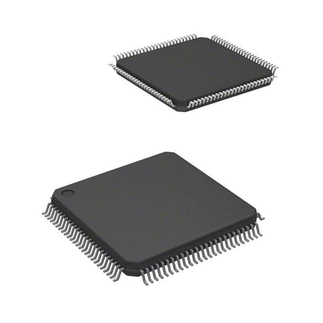
STM32F407VET6 STMicroelectronics MCU Selection Guide
STM32F407VET6 guide covering Cortex-M4 use, 512KB Flash, LQFP100 pinout checks, alternatives and sourcing notes.
-
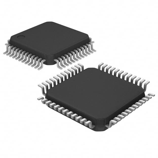
STM32F103C8T6 STMicroelectronics MCU Selection Guide
STM32F103C8T6 guide covering Cortex-M3 use, 64KB Flash, LQFP48 pinout checks, alternatives and sourcing notes.
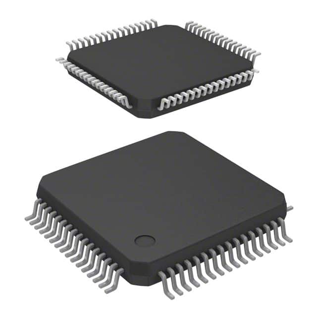
-
STM32F405RGT6 STMicroelectronics MCU Selection Guide
STM32F405RGT6 guide covering Cortex-M4 use, 1MB Flash, LQFP64 pinout checks, alternatives and sourcing notes for engineers.
-1,80mm.jpg)
-
GRM31CR61H106KA12L Murata MLCC: Applications, Selection and Buying Notes
GRM31CR61H106KA12L Murata MLCC guide for 10uF 50V X5R 1206 use, obsolete-status review, alternatives and sourcing checks.
-
GRM31CR61E476ME44L Murata MLCC: Applications, Selection and Buying Notes
GRM31CR61E476ME44L Murata MLCC guide for 47uF 25V X5R 1206 decoupling, alternatives and sourcing confirmation.
-2,70mm.jpg)
-
GRM32ER71H106KA12L Murata MLCC: Applications, Selection and Buying Notes
GRM32ER71H106KA12L Murata MLCC guide covering applications, selection, alternatives and sourcing checks for 10 uF, 50V, X7R, +/-10%, 1210 MLCC.
-0,55mm.jpg)
-
GRT155C81E105KE13D Murata MLCC: Applications, Selection and Buying Notes
GRT155C81E105KE13D Murata MLCC guide covering applications, selection, alternatives and sourcing checks for 1 uF, 25V, X6S, +/-10%, 0402 automotive MLCC.
-
GRM155C81E105KE11D Murata MLCC: Applications, Selection and Buying Notes
GRM155C81E105KE11D Murata MLCC guide covering applications, selection, alternatives and sourcing checks for 1 uF, 25V, X6S, +/-10%, 0402 MLCC.
Related Products
-
FAN53601AUC105X
onsemi
-
MIC23250-SKYMT-TR
Microchip Technology
-
TPS63002DRCTG4
Texas Instruments
-
AP1604AWG-7
Diodes Incorporated
-
FAN48617UC50X
onsemi
-
FAN48610BUC33X
onsemi
-
FAN48611UC53X
onsemi
-
FAN48615UC11X
onsemi
-
BM2P093
Rohm Semiconductor
-
MPQ2178AGQHE-AEC1-Z
Monolithic Power Systems Inc.
-
TPS61010DRCR
Texas Instruments
-
TPS61013DGSR
Texas Instruments


