Free Shipping Over$200

- Products
- Marking
- Alternative

Adding Protection Parts to Interfaces and Power Inputs
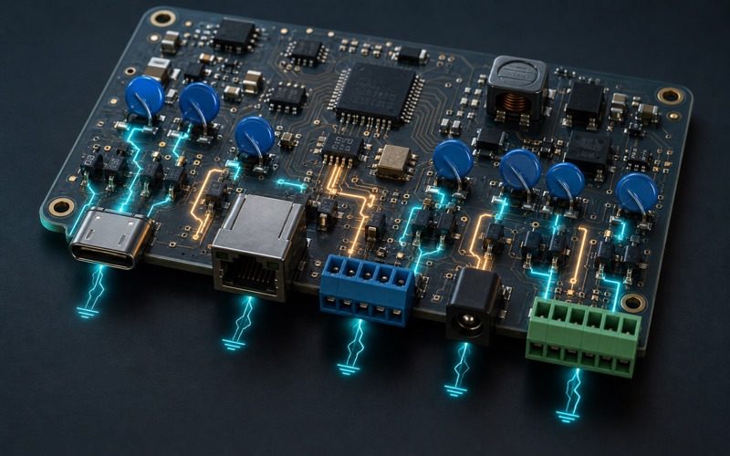
Protection parts are often added late, after the connector and main circuit already look finished. That order creates weak products. The outside world enters through a few places: a power jack, a USB port, a terminal block, a sensor cable, a user touch point or a service header. Those openings carry surge, ESD, reverse wiring, overvoltage, hot plug current and cable noise toward the board. A small clamp symbol near the connector is not enough. Protection has to be part of the interface architecture.
P3.27 groups passive clamps and active input protectors by the stress they handle. Varistors absorb or clamp higher energy transients. TVS diodes clamp fast voltage events on power or slower signal lines. Low capacitance ESD parts protect data lines without ruining the signal. eFuses and current limited switches shape fault current, startup and recovery. The right part is chosen by the entry point, the allowed signal loading, the energy level, the ground path and the fault behavior the product can tolerate.
The connector edge is the protection boundary
The first design rule is physical. Connectors belong on the board edge with openings facing outward, so the cable enters from outside the board rather than pointing into the component field. Protection parts then sit just behind that edge, before the trace has a chance to cross the board. If the clamp sits deep inside the layout, the discharge current already traveled through copper that may pass under a processor, radio, ADC or memory bus. The schematic may show protection, but the board allowed the event to spread.
CU3225K250G2 as a multilayer varistor belongs at this boundary. A multilayer varistor can be useful where a compact clamp is needed near an entry point and the signal or supply can accept its capacitance and leakage. It should be checked against working voltage, clamping voltage, pulse rating, capacitance and aging under repeated events. A varistor is not a universal ESD answer. It has a voltage-current curve, parasitic capacitance and wear behavior that must fit the node.
V300LA4P as a metal oxide varistor points to higher energy line protection. A metal oxide varistor can sit across an AC or higher voltage input to clamp surge energy, often with a fuse, thermal element or upstream impedance as part of the protection scheme. It should be sized by the line voltage, surge environment, energy rating, follow current risk and end-of-life behavior. The question is not only whether the part survives one event. The product must fail in an acceptable way after repeated stress.
TVS selection is a voltage, energy and layout problem
SZ1SMA28CAT3G as a transient voltage suppressor fits the TVS discussion for power and slower interface lines. A TVS diode is chosen from standoff voltage, breakdown voltage, clamping voltage, pulse power, package inductance and leakage. The selected standoff voltage must stay above the normal operating voltage across tolerance and temperature. The clamping voltage must stay below what the downstream circuit can survive under the defined pulse. Those two limits often pull against each other.
SMAJ48CA-E3/61 as a bidirectional TVS diode is a different fit when the line can swing positive and negative, or when polarity at the protected node is not fixed. Bidirectional parts are common around AC, differential pairs with common-mode stress, and interfaces where either direction of transient has to be clamped. The designer still has to check the working voltage and capacitance. A bidirectional TVS can be the wrong part for a fast data line even if it is the right idea for a power entry.
Layout decides whether the TVS does the job. The clamp path to chassis, shield or ground has to be short and wide, with the protected trace passing the clamp before it reaches sensitive circuitry. A long thin branch to a TVS adds inductance. During an ESD edge, that inductance creates voltage. The board may pass a static review and fail in the lab because the current path formed a loop around the device that should have been protected.
Ground strategy has to be explicit. A connector shield may go to chassis or a quiet reference through a controlled network. A TVS may return to power ground. A data-line ESD array may need a low impedance path to the local return. If every clamp dumps current into the same narrow digital ground neck, the protection event becomes a reset event. Good protection does not only clamp voltage at the pin. It gives surge current a route that avoids the logic core.
Fast data interfaces need low capacitance protection
ESD5304D-10 as a low capacitance ESD protector belongs near USB, sensor buses and other interfaces where extra capacitance can close the eye, slow the edge or disturb impedance. Low capacitance ESD parts trade energy handling and capacitance in a way that must match the data rate and exposure level. The data sheet capacitance is not decoration. It is part of the channel budget, just like connector footprint, via stub and trace length.
D20V0L1B2WS-7 as an ESD protection diode covers a smaller single-line protection role. A one-line ESD diode can be enough for a button, GPIO, low speed control, identification pin or touch-accessible node. It still needs placement discipline. The diode should be closer to the entry than the protected IC. The return via should be close. The trace should not pass the IC first and then visit the protector on the way back.
ESD protection is easy to overfit to a lab level. A device may pass IEC contact discharge on one port and fail when a cable is attached to a different port, or when a user touches a metal shell connected through an unexpected path. The protection plan should mark every user-accessible conductor, every cable shield, every removable connector and every production test pad. If a finger, cable, fixture or tool can touch it, it has to be placed into the ESD map.
Active protection controls current and recovery
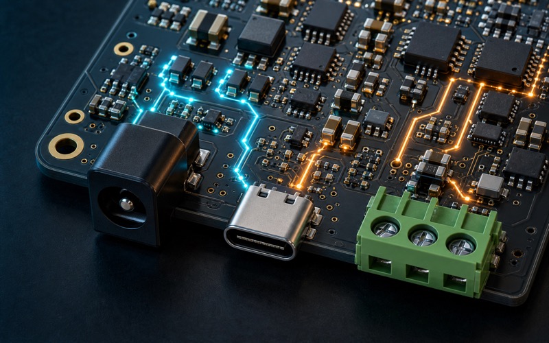
Passive clamps handle voltage stress, but many power faults are current problems. TPS259570DSGR as an eFuse with overvoltage protection belongs on the active input protection side. An eFuse can limit inrush current, turn off during overcurrent, block or manage overvoltage, report fault state and allow controlled restart. It is useful where a power input may be hot plugged, miswired, overloaded or exposed to adapters that do not behave the same way.
The eFuse should be chosen by normal load, startup capacitance, short-circuit current, thermal response, retry behavior, fault signaling and downstream regulator tolerance. A current limit that is too low creates false trips during radio transmit or motor startup. A current limit that is too high lets a connector, cable or downstream trace carry more energy than it should. The fault response must match the product. Some systems should latch off until firmware or a user resets them. Some should retry with a controlled duty cycle. Some should report the fault before shutdown.
AP22653AFDZ-7 as a load switch with current limit is a smaller active control element. A current limited load switch can gate a USB peripheral rail, sensor power domain, module rail or external accessory supply. It lets the controller turn a rail on, limit a fault, and sometimes read an overcurrent flag. It is not the same as a plain MOSFET. The current limit, enable threshold, reverse current behavior, thermal shutdown and output discharge path all change how the rail behaves during a fault.
Active protectors need firmware ownership. If a fault pin is ignored, the system loses diagnostic value. If an enable pin floats during reset, the rail may turn on at the wrong time. If firmware retries a fault too quickly, a damaged cable can heat. If a load switch feeds an external connector, the product should define what happens when the connector is shorted before power-up, shorted during operation, and removed during a fault. Hardware can limit damage, but system behavior finishes the protection story.
Protection is verified as a path, not as a part
The selection checklist should start at the entry. What can be connected? What voltage, polarity and cable length can appear? What surge or ESD standard matters? Where does the shield current go? What node is allowed to clamp, fold back, latch off or reset? Which line is high speed and cannot tolerate much capacitance? Which power input needs inrush control? Which fault must firmware see?
After those answers, each part can be judged in context. A varistor needs working voltage and energy margin. A TVS needs the right standoff, clamp and return path. A low capacitance ESD array needs data-channel review. An eFuse needs current limit and recovery behavior. A load switch needs enable logic and thermal behavior. The part number alone does not prove protection. The board path, the ground return and the system response prove it.
Substitution should be treated with the same discipline. A different varistor may share size and working voltage while changing capacitance, clamp level or pulse lifetime. A different TVS may have a better power rating but a higher clamp voltage at the pulse current that matters. A lower capacitance ESD part may protect the signal quality and give up surge margin. An eFuse with a similar current limit may use a different blanking time, thermal shutdown point or retry mode. A load switch may discharge the output in one version and leave it floating in another. Pin compatibility is only the start of the review.
Production and service add more cases. A test fixture may touch a header before the enclosure shield is installed. A field installer may land a cable on the wrong terminal. A service cable may connect ground before signal, or signal before ground. A user may unplug a live accessory and create an arc at the contact. A bench supply may current-limit during startup and make the eFuse behave in a mode that the final adapter never uses. These cases should be written into the validation plan because they are the events that turn a good schematic into a support ticket.
The recovery state is as important as the survival state. After an ESD hit, the product should still enumerate, measure, communicate or restart in a known way. After a shorted accessory, the load switch should cool and report the condition. After an overvoltage event, the eFuse should keep the downstream rail inside the allowed range or shut it off. After a surge clamp, the fuse, varistor and TVS should be inspected for damage mode and leakage change. A pass that leaves the device half alive is not a pass for a deployed product.
Bench testing should include wrong adapter, current-limited adapter, hot plug, cable removal, output short, ESD at every user-accessible point, and a normal operation run right after the stress. The product should not only survive. It should recover in the intended state, keep data where needed, avoid a hidden latch-up and report faults that the user or firmware can act on. Good interface protection is quiet in normal use, decisive during a fault and honest during recovery.