Free Shipping Over$200

- Products
- Marking
- Alternative

Choosing a Thermal Interface Material That Earns Its Place
Choosing a Thermal Interface Material That Earns Its Place
A thermal interface material earns its place only when it fixes a contact problem that the metal stack cannot fix by itself. If the package, heat spreader and heatsink already touch with controlled pressure, adding a thick pad can make the path worse.
The useful question is physical: what gap must be filled, how flat are the two surfaces, how much pressure is available, what electrical isolation is needed and what happens after heat cycles, vibration and service. Conductivity on a label cannot answer those questions alone.
Start With the Gap the Material Must Fill
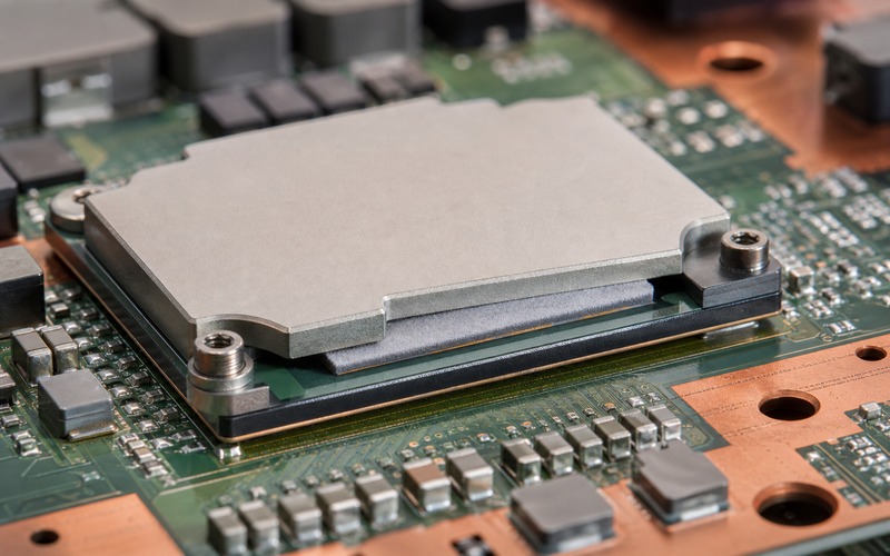
The first decision is geometry. A material that works across a small flat lid may fail across a taller package, a tilted heat spreader or a board stack with uneven screw force. Measure the nominal gap, the tolerance stack and the part-to-part variation before choosing the form.
Gap size decides the material family. A paste or phase-change film can suit a thin controlled interface. A soft pad or gap filler can bridge package height differences and nearby component steps. A graphite sheet may spread heat well in-plane but still needs contact pressure and electrical review.
Do not size the pad from the best sample. The release stack should include package tolerance, board warp, heat-spreader flatness, screw height, adhesive thickness and enclosure tolerance. If the pad is thin enough only in the cleanest build, production will create uneven contact.
Coverage needs the same discipline. A pad that misses a hot corner, extends over a keepout, touches an exposed node or rides on a package edge can create a local hot spot or an electrical risk. The shape should come from the real package and mounting stack, not from a rectangular placeholder.
Separate Conductivity From Installed Resistance
The catalog conductivity value is a material property under test conditions. The product cares about installed thermal resistance: material thickness, contact area, pressure, surface roughness, voids, pump-out, aging and how heat spreads after it leaves the package.
A thinner material with lower listed conductivity can outperform a thicker high-conductivity pad if the thin interface reaches better contact and covers the active heat area. A thick pad can solve tolerance and dielectric needs while adding resistance, so the trade must be tested in the stack.
Pressure changes the result. Too little pressure leaves air gaps, which are poor heat paths. Too much pressure can crack parts, bend the board, push material out, damage solder joints or overload clips and screws. The selected material should work inside the force the product can apply repeatedly.
Surface finish matters as well. A milled heat spreader, stamped metal plate, anodized surface, plated copper area and molded package top do not present the same roughness or flatness. The interface material must be matched to the real surfaces it will see.
Thermal spreading should be included in the resistance path. If heat leaves a small silicon area and enters a larger spreader, the material must cover the active zone and the spreader must carry heat away without choking at the edges. A pad that looks large enough in outline can still miss the real heat source when die position, package layout and mounting offset are considered.
Use a short resistance budget to avoid wishful selection. Start with the allowed rise from ambient or internal air to junction, subtract the known package path, estimate the heat-spreader and heatsink path, then assign the remaining margin to the interface. The calculation will be rough, but it shows whether a thick cushion can fit the thermal target or whether a thinner controlled interface is needed.
Choose the Form by Assembly Reality
Grease can fill fine surface texture, but it needs process control and can migrate or contaminate sensitive areas. Phase-change material can reduce handling mess, yet it still needs pressure and temperature to wet the surfaces. A pre-cut pad is easier to place, while thickness and compression dominate its result.
Gap fillers help when the mechanical stack cannot guarantee a small gap. They need placement control, cure or dispense control when applicable, and limits on squeeze-out. A material that flows into nearby connectors, optical areas, microphones or test pads can create a production issue even when the thermal result is acceptable.
Graphite, foil and spreader sheets can move heat laterally, but they introduce handling, isolation and edge-clearance questions. They may help when the hot spot must be spread before reaching the enclosure, yet they should not be used as a shortcut around poor vertical contact.
Pick the form that the factory can repeat. Operator placement, liner removal, automated dispensing, shelf life, storage humidity, cure time, rework path and inspection method decide whether the thermal design survives production.
Check Electrical and Mechanical Side Effects
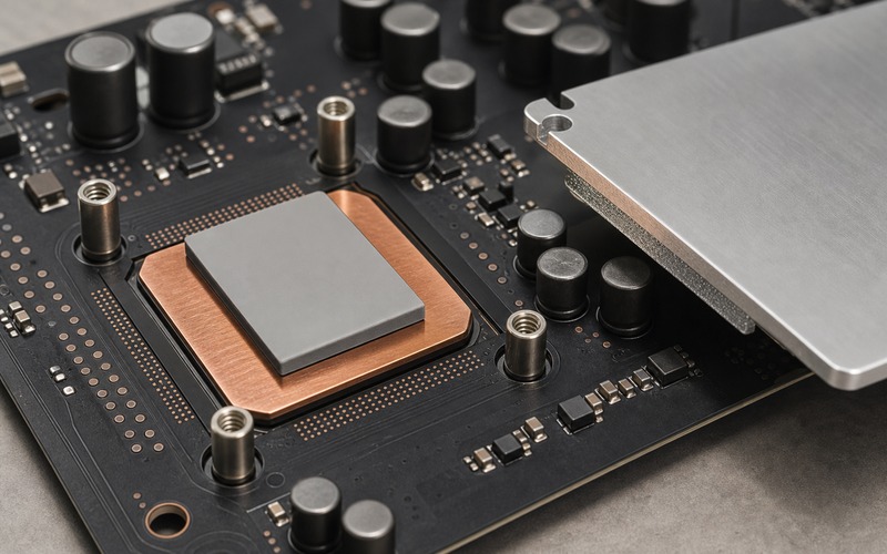
Thermal materials sit close to power rails, package pins, exposed copper and shields. Dielectric strength, breakdown margin, volume resistivity and edge clearance can matter as much as heat flow when the material crosses electrical features.
A conductive material may be acceptable under a grounded heat spreader and dangerous near exposed nodes. An insulating pad may protect the circuit but add thickness or resistance. The selection should state whether the interface is electrically insulating, electrically conductive or tied to a controlled potential.
Mechanical stress can decide reliability. Compression set, creep, pump-out, abrasion and vibration can change contact after thermal cycling. A soft pad that looks perfect on day one may relax. A hard pad can protect thickness but transfer force into solder joints and package corners.
Contamination belongs in the review. Oils, fillers, silicone bleed, particles and residue can affect optics, microphones, connectors, relays or conformal coating. If the board sits near a camera, MEMS microphone, optical sensor or high-impedance analog node, material cleanliness should be treated as a real requirement.
Service behavior matters for long-life equipment. When a heat spreader is removed, some materials tear, leave residue or need full replacement. A field-serviceable product needs a clear rule for reuse, replacement, cleaning and torque; otherwise repair work can silently reduce thermal margin.
Place the Material Around the Real Heat Source
Package outline does not always match heat location. Some processors have uneven die placement, memory stacks, chiplets, hot I/O banks or a package lid that spreads heat before the interface. If the pad is centered only on the package rectangle, it may miss the area that needs pressure.
Nearby components create layout boundaries. Tall capacitors, inductors, connectors and shields can limit heat-spreader shape or screw placement. A pad that collides with a component, covers a test point or traps rework access will cause trouble after the first build.
Copper below the package should be planned with the interface above it. Thermal vias and copper pours can move heat through the board, but they can also warm sensors, memory or regulators. The material choice should match the intended heat exit: up into a spreader, down through the board or sideways into enclosure metal.
Keep the pad shape inspectable. A hidden interface that cannot be checked after assembly needs placement features, process controls or a sample audit. If operators cannot see whether the pad folded, shifted or trapped a liner, the design depends on luck.
Validate With the Final Stack
Bench coupons help compare materials, but the release decision belongs to the product stack. The test needs the real package, board revision, copper, spreader, screws or clips, enclosure, assembly torque, pad thickness and workload.
Measure before and after warm soak. Record the accelerator thermal sensor or estimate, spreader temperature, nearby board temperature, power-stage temperature, enclosure surface and performance state. If the workload throttles or latency shifts, the interface is part of the system behavior.
Test enough builds to see variation. One hand-built sample with fresh material and careful pressure can hide tolerance. Try samples with normal assembly, edge-of-tolerance gap and rework if rework is allowed. The material must survive the range the factory will produce.
Use comparison tests carefully. Changing the pad, heat spreader and screw force at the same time may hide which item improved the result. Hold the stack constant when comparing material families, then retest the final combination as a system.
Visual inspection after disassembly can explain failures. Dry spots, trapped liners, torn corners, squeeze-out, pump-out, imprint patterns and uneven compression show whether contact matched the drawing. Keep photos with the thermal data so future substitutes can be judged against evidence.
Keep the inspection tied to assembly time as well as temperature. A pad that shifts during lid placement, picks up dust from a liner, or bridges a nearby keepout may still give one acceptable temperature result. The same defect can later create leakage, unstable contact or a field-service problem. The release record should connect thermal data, build method and post-test appearance.
Set a Controlled Substitute Boundary
A substitute material cannot be approved by color and thickness alone. The boundary should include material family, conductivity range, thickness, tolerance, hardness or compressibility, dielectric behavior, operating temperature, flammability class when required, liner handling and shelf-life limits.
Geometry is part of the boundary. Cut size, corner radius, hole pattern, edge clearance, adhesive side, release liner and orientation features affect placement. A supplier change that shifts hole position or edge overhang can change both contact and safety clearance.
Requalification should repeat the installed test rather than stop at a data-sheet comparison. Check warm-soaked performance, spreader temperature, local board temperature, surface temperature, visual compression pattern and rework result. If the product has acoustic, touch or reliability limits tied to temperature, include them.
Keep the approved list short. A wide open substitute list invites visually similar materials that do not share compression behavior or residue profile. Purchasing needs exact boundaries so a shortage does not turn into a hidden thermal redesign.
Thermal Interface Release Checklist
Before release, check gap range, flatness, pressure, material family, thickness, compression, coverage, die location, copper spreading, thermal vias, dielectric need, contamination risk, service rule, shelf life, placement method, inspection path and allowed substitute boundary.
Then verify the installed result. The material is ready when the hot part, spreader, board and enclosure hold the workload after warm soak, the contact pattern is repeatable and the mechanical stack can be built without damaging nearby components.
A thermal interface material should remove air from the heat path without adding a new problem. If it hides a bad gap, blocks service, raises stress or depends on a perfect sample, it has not earned its place.
Related information
- 2026.07.08 A Wide Voltage Input for an Edge Box
- 2026.07.08 The Design Limits of a Fanless Edge AI Box