Free Shipping Over$200

- Products
- Marking
- Alternative

Decoupling Around a High Current Processor
Decoupling Around a High Current Processor
A high current processor does not wait politely for a distant regulator. It asks for charge in short edges, through a package, across planes, through vias and into transistor banks that switch in groups. If the local capacitors are placed as decoration around the chip, the rail can look correct at a meter point and still collapse at the silicon. Decoupling around that processor is a layout decision first, then a capacitor value decision.
The schematic usually hides the hard part. It may show many capacitors tied between a core rail and ground, with several values repeated around the processor. That drawing does not say which capacitors touch the package edge, which ones share a via path, which ones sit behind a plane neck, which ones serve a memory rail instead of a core rail, or which ones are too far away to help a fast current edge. The released board needs a placement rule that purchasing and layout can preserve, not a loose pile of values.
Start at the Current Loop
The first question is where the transient current loop closes. A capacitor placed beside the processor is useful only if its current can leave the rail, enter the package area and return through a short ground path. The loop includes capacitor pads, mounting inductance, vias, plane spreading, package balls and the internal power grid. A larger capacitance value cannot compensate for a long narrow path when the edge rate is fast.
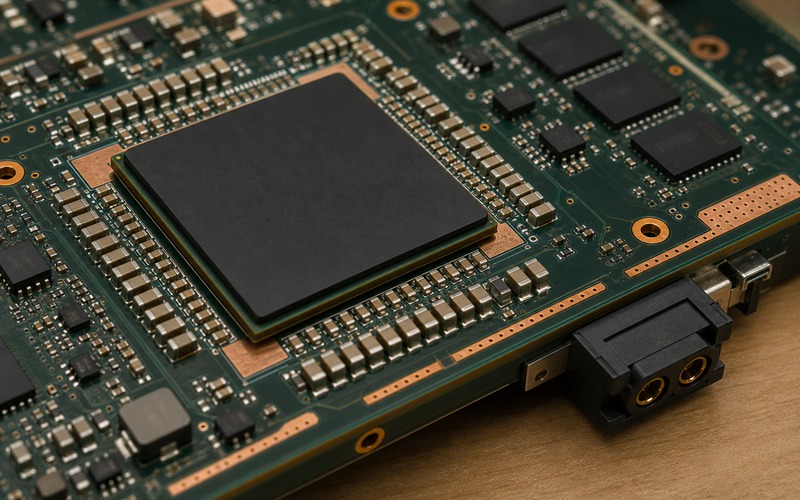
Place the smallest, fastest decoupling parts close to the rail pins they support. For a BGA processor, that often means capacitor rows just outside the package, via-in-pad or tight via pairs where the fabrication rules allow them, and power-ground plane pairs with short spreading distance. The goal is not to make the board look full. The goal is to create many short, low-inductance paths from the rail to the die.
The return path deserves the same attention as the rail path. If the ground via for a capacitor sits far from the power via, the loop area grows. If a split, slot, connector cutout or dense signal fanout forces current around an obstacle, the capacitor becomes less effective than its value suggests. The layout review should follow current rather than component outlines alone.
Place First Capacitors at the Package Edge
The first capacitor ring should be treated as part of the processor footprint. It should be protected in the layout rules, in the assembly drawing and in any future replacement discussion. Moving those parts outward to make room for a label, test point, mounting hole or late signal escape can change the rail response even when the bill of materials stays unchanged.
For each rail, group the close capacitors by the pins they serve. Core, memory, analog, PLL, I/O and auxiliary rails may need different locations and different noise boundaries. A clean drawing labels the rail zone by function, then places the closest capacitors where the current path makes sense. It avoids a mixed border where a technician cannot tell which rail a given capacitor is protecting.
Capacitor orientation matters when pad and via geometry decide the loop. A row of MLCCs rotated for neat alignment can have a longer current path than a less tidy row pointed toward the rail via field. When the processor pulls current, the board does not care whether the row looks symmetrical. It cares about path length, shared vias, plane entry and return current.
There is also a manufacturing limit. Parts packed too tightly can complicate inspection, rework, solder fillet visibility and tombstoning risk. A good placement gives the electrical path priority while leaving enough assembly margin for the package class, solder paste process and board finish. The design file should state which capacitors are position-critical and which ones can move if assembly feedback demands it.
Separate Bulk, Mid and High Frequency Roles
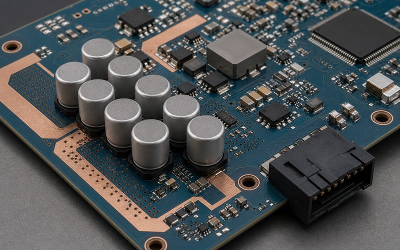
Different capacitors serve different parts of the load event. Small MLCCs near the package handle fast edges and local high-frequency current. Mid-size MLCCs and local banks support lower-frequency movement and damp rail movement over a larger area. Bulk capacitors near the regulator or rail entry support longer load steps, cable effects and converter response. Treating all capacitance as one total number hides this timing difference.
The values should not be chosen as a decorative decade spread. Review the processor vendor guidance, regulator stability range, target impedance, rail tolerance, package pins, plane pair geometry and load profile. If the board uses many values, check whether anti-resonance creates a peak in the rail impedance. A rail can have enough total capacitance on paper and still ring at a frequency that the processor excites.
Voltage bias changes MLCC value. A nominal capacitor may lose a large share of effective capacitance under DC bias, and that loss depends on dielectric, case size, voltage rating and manufacturer series. The released bill of materials should carry enough detail to preserve effective capacitance instead of preserving the printed value alone. Substituting a smaller case or a lower voltage rating can change the rail even when the nominal value matches.
ESR and ESL matter as much as capacitance in the close ring. A capacitor with a low effective series inductance helps only if the mounting path does not add the inductance back through long traces or shared vias. The layout and the part selection must be reviewed together, because the capacitor data sheet and the PCB geometry form one network.
Watch Via Inductance and Plane Geometry
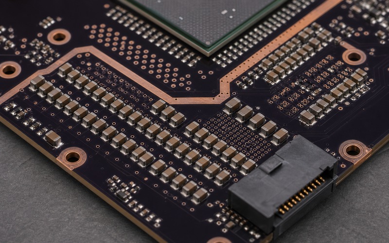
A processor rail often enters through several vias, plane islands and narrow necks before it reaches the package. Those features become part of the decoupling system. If a capacitor bank connects to a broad copper pour that narrows before the BGA field, the broad copper may look comforting while the neck sets the real impedance. The same problem appears when a dense signal breakout cuts the power plane into thin fingers.
Via count helps only when the vias land in useful locations. A field of vias far from the capacitor pads or blocked by another layer transition may not serve the fast loop. Use paired power and ground vias near each close capacitor where possible, keep the path short, and check whether the via field reaches the correct internal plane pair. Blind, buried or microvia choices should match fabrication capability and reliability requirements.
Plane pair spacing affects capacitance and spreading inductance. A tight power-ground pair near the processor can support local transient current better than a distant pair separated by thick dielectric. That does not remove the need for discrete capacitors, but it changes how the board carries current between the package and the capacitor network. Stackup review belongs in the decoupling decision.
Thermal design can disturb the same area. Large copper, thermal vias, heat spreaders and mounting holes may compete with power integrity routes. A thermal opening that removes copper near the processor can weaken a rail path. A decoupling rule that ignores thermal copper may pass the schematic check and fail the physical board review.
Keep Memory and Clock Noise Out of the Rail Decision
High current processors rarely sit alone. Memory packages, oscillators, interfaces and power converters crowd the same area. The decoupling plan should protect each rail without letting noisy current run through sensitive neighbors. A memory rail capacitor should not borrow a return path that shakes an analog reference or a clock island. A core rail capacitor should not force a high-current loop under a high-speed interface escape.
Clock and PLL supplies need special care. They may draw less current than the core rail, but they can be sensitive to noise from the processor, memory and switching regulators. Keep their local filtering and decoupling close, keep the return path quiet, and avoid placing those parts where a high-current core rail loop crosses the same copper.
Memory rails have their own transient behavior. A shared power plane between processor and memory can be efficient, but it also couples load movement between devices. Check the placement of memory decoupling, termination power if used, and the route from the regulator to both loads. A board that runs at room temperature during bring-up can still show margin loss during hot, high-bandwidth operation.
Give Purchasing Real Decoupling Boundaries
Decoupling parts are often treated as easy substitutions because they look generic. That is risky near a high-current processor. The purchase boundary should state value, tolerance, voltage rating, case size, dielectric, temperature class, preferred series and approved alternates. It should also say which capacitors are position-critical and which values must be kept together as a network.
Do not approve an alternate by nominal capacitance alone. Check DC bias behavior, impedance curve, package size, height, termination type, aging behavior and temperature behavior. If a vendor change affects the close ring, the board should be checked with the same rail measurement points used during release. A harmless-looking MLCC change can move a resonance peak or reduce effective capacitance under the actual rail voltage.
Assembly changes need review as well. Paste aperture, tombstoning risk, reflow profile, board finish, cleaning process and inspection access can affect dense capacitor rows. A design that relies on tight placement must still be buildable at volume. If production moves a capacitor for yield, the electrical owner needs to approve the new loop path.
The drawing should separate flexible capacitors from fixed capacitors. Bulk parts near the rail entry may allow small movement if the copper area and measurement result remain acceptable. The first ring beside the processor often has less freedom. Marking that difference prevents a later layout cleanup or alternate footprint request from weakening the part of the network that handles the fastest current edge.
Test access also belongs in the boundary. A rail measurement taken at a regulator output can miss the voltage seen at the processor. Keep a low-inductance measurement point near the load area, record the probe method, and repeat the same method after a capacitor family, case size or placement change. Without that discipline, two boards can appear comparable while their local rail behavior is different.
Final Processor Decoupling Checklist
Before release, check each processor rail against the pin group it serves, close capacitor placement, via pairing, effective capacitance under bias, voltage rating, dielectric, case size, impedance behavior, anti-resonance risk, plane pair spacing, rail entry geometry, regulator stability range, memory interaction, clock and PLL isolation, assembly clearance, rework access and approved alternate list.
Keep the evidence with the board file. Include placement screenshots, stackup notes, rail measurement points, load-step waveforms, thermal notes, allowed capacitor series and any movement limits for the first capacitor ring. That record gives layout, engineering, purchasing and production the same boundary. A high current processor will expose weak decoupling through resets, compute throttling, memory errors, clock sensitivity or field failures. The board has a better chance when the capacitor network is treated as part of the processor power path, not a scattered list of passive values.