 Free Shipping Over$200

- Products
- Marking
- Alternative

MX25V1006FZUI as a Small Density SPI Flash
MX25V1006FZUI as a Small Density SPI Flash
The MX25V1006FZUI is a 1-megabit serial NOR flash for boards that need a small, separate nonvolatile store rather than another multi-megabyte device. One megabit is 131,072 bytes, or 128 KiB. The exact ZUI suffix identifies a 2 x 3 mm 8-USON package rated from -40 to +85 C. The device operates from 2.3 to 3.6 V, supports single- and dual-I/O serial reads, and reaches 104 MHz when the supply is at least 2.7 V.
That small capacity changes the design question. This part can hold a compact boot stage, a recovery image for a small controller, factory configuration, calibration tables, immutable lookup data or a protected set of product parameters. It is a poor fit for a large Linux image, a modern vision model or two full application images. Capacity must be budgeted in bytes before the package is approved, because a nominal density says nothing about headers, signatures, rollback data, journals or safe update space.
The selection review also has to cover erase geometry, page programming, write endurance, power interruption, deep power-down, protection bits and the hidden-land USON footprint. A substitute with the same density may differ in voltage range, read commands, pin functions or erase opcodes. The practical goal is a storage path that can be programmed in production, updated without corrupting its only valid copy, and verified after every cold start.
Read the Complete Ordering Code
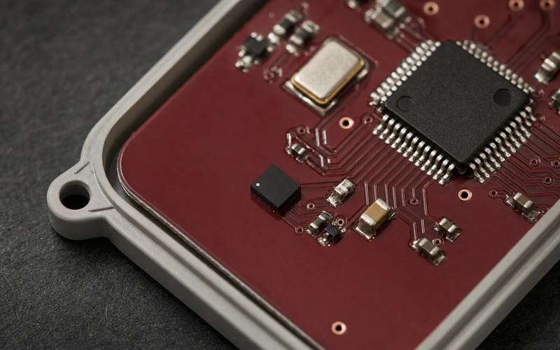
MX25V1006F names the 1Mbit serial NOR family. In MX25V1006FZUI, ZU selects the 2 x 3 mm 8-USON package and I selects the industrial -40 to +85 C temperature range. That suffix belongs in the approved BOM, footprint library, programming setup and incoming inspection rule. Treating the base family as the orderable item can bring in a TSSOP or SOP that cannot fit the board.
The package has eight lands but one position is not connected in this version, and the family does not provide the HOLD# function used by some older serial flash designs. Pin 1, write protect, clock, chip select, power and the two serial data signals must come from the exact drawing. A pin-compatible appearance does not prove that the unused or control pins behave the same way.
Decide Whether 128 KiB Is Enough
Start with a byte-level map. List the executable image, vector table, metadata, signature, device configuration, calibration records, manufacturing identity and recovery information. Add alignment and erase-sector losses. A 96 KiB application may appear to fit, but it leaves little room for a second image, a rollback marker or a journal once the 4 KiB erase unit is respected.
A small external flash works well when its responsibility is narrow and stable. Examples include a signed first-stage loader, a golden configuration for an FPGA or peripheral, language-independent lookup tables, calibration data copied into RAM, or a compact controller image that is replaced through a wired service procedure. Write down what the part does not store as carefully as what it does store.
Choose a Safe Update Layout
An update design needs at least one known-good image while new data is received and checked. With only 128 KiB, two equal application slots may be impossible. A better architecture may keep the main application in internal MCU flash and use this device for a compressed recovery payload, signed patch, configuration journal or immutable factory image. The choice follows from the actual image sizes and recovery path.
Every record that changes should carry a format version, length, sequence number and integrity check. Write the new record into erased space, read it back, verify it, then change a small activation marker. Do not erase the previous valid record until the new one has survived verification and a reboot. This sequence turns limited capacity into a recoverable system rather than a single fragile copy.
Match the Supply and Logic Levels
The specified operating range is 2.3 to 3.6 V. A 3.3 V rail is straightforward, while a nominal 2.5 V rail reduces the maximum fast-read clock to the lower-voltage limit. The device is not a 1.8 V flash, so a low-voltage processor bank needs either a compatible I/O rail or level translation whose direction and startup state are understood.
Place about 0.1 uF of local decoupling close to VCC and ground, using the manufacturer's power-up guidance as the starting point. Keep CS# high while the rail rises or falls, normally with a pull-up that is valid even when the processor is unpowered. Shared rails must avoid back-power through SCLK or data pins during programming, sleep and board-level test.
Use the Right Serial Read Mode
The part supports ordinary single-I/O reads and dual-output or dual-I/O reads. It is not a quad-I/O device. At 2.7 to 3.6 V, fast reads can operate at 104 MHz with the specified dummy cycles; from 2.3 to 2.7 V, the limit is 80 MHz. The controller setup must match the command, bus width, dummy clocks and voltage corner used in the product.
Read speed should be measured with the real workload. Command overhead, chip-select gaps, software copies and small random transfers can dominate a 128 KiB device. Begin at a conservative clock, verify the JEDEC identity, read a known pattern across page and sector boundaries, then raise the frequency while testing voltage, temperature and production board variation.
Respect Pages, Sectors and Blocks
Programming operates on pages up to 256 bytes. Erase operates on 4 KiB sectors, 32 KiB blocks, 64 KiB blocks or the whole device. Those units shape the data layout. A one-byte configuration change can require preserving and rewriting an entire 4 KiB sector unless the firmware uses an append-only journal or multiple rotating records.
NOR programming changes erased ones to zeros. Returning a zero to one requires an erase. Before a page program, the driver sets write enable, checks that the target is erased, sends data without crossing an unsupported page boundary, and polls the write-in-progress bit to completion. Erase and program operations also need timeout and verification paths rather than a fixed delay.
Budget Program and Erase Time
The datasheet gives a typical 1.6 ms page-program time and a typical 50 ms 4 KiB sector erase time under its stated conditions. Maximum times are longer, especially at voltage and temperature corners and after cycling. A watchdog, boot-time target or field-service tool must use the guaranteed limits and poll status instead of assuming the typical number.
Large block or chip erase can pause access for much longer than a page write. If the host executes from the same serial bus or shares it with another device, coordinate access and interrupt behavior. Production tools should program only the intended ranges, verify every written byte, and avoid a chip erase when preserving factory data or unique configuration.
Design for Endurance and Retention
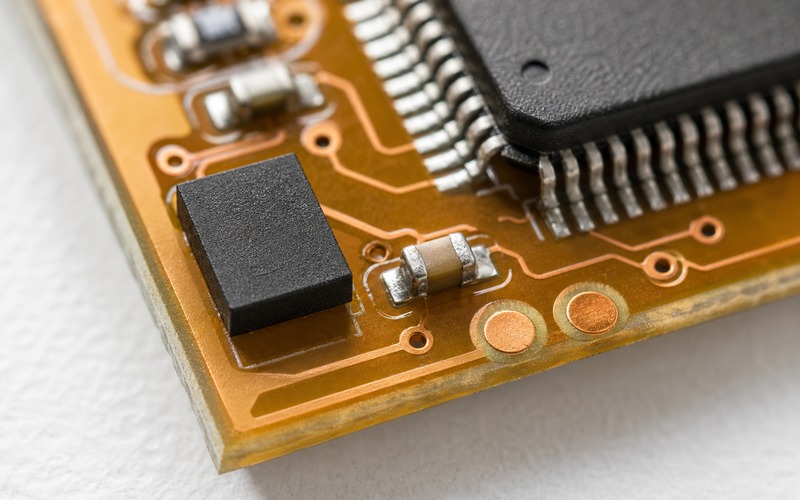
The family specification states at least 100,000 erase/program cycles and 20 years of data retention at the stated condition. Those figures apply to the memory technology, not automatically to a repeatedly rewritten parameter stored in one sector. A counter updated every second would consume one location quickly even though most of the array remains unused.
Use sequence-numbered records across several sectors for settings that change. Compact old records only when a sector is full, and keep a separate immutable factory copy where appropriate. Estimate writes from the real duty cycle, service life and worst operating temperature. For long retention, include readback or integrity checks during maintenance and provide a controlled refresh path.
Use Deep Power-Down Deliberately
Typical standby current is 5 uA and typical deep-power-down current is 1 uA. That difference can matter in a sensor node that sleeps for months, but the saving is real only if firmware enters the mode after every transaction and accounts for the release sequence and wake time. A device in deep power-down will not answer ordinary read commands.
Define who owns the flash state when several software layers share the SPI bus. The boot loader, application, update service and diagnostic code need one rule for entry, release and reset. Measure board current with the processor pins in their actual sleep states, because pull resistors, level shifters and another device on the bus can consume more than the flash itself.
Protect Code and Configuration
Status-register block-protection bits can protect selected regions against program and erase, and WP# can add hardware control when the status-register protection mode is configured correctly. These mechanisms reduce accidental writes. They do not replace image authentication, encryption or secure key storage when the product has a security requirement.
Lock the region holding the recovery loader or factory constants after programming, then verify the protection by attempting an expected rejected operation on a test unit. Document how an authorized update temporarily changes protection and restores it after verification. On reset, firmware should read the status register instead of assuming the previous protection state survived every event.
Handle Power Failure and Reset
Power loss during program or erase can leave the target data uncertain. The design should prevent a falling supply from starting a new write, hold CS# inactive, and give firmware enough monitored energy to finish or abandon an operation safely. Redundant records and activation markers are still required because no capacitor can cover every unplug, brownout or battery contact event.
The software-reset sequence returns volatile settings to their power-on state, but issuing reset during an active program or erase can damage the data being processed. Poll WIP before reset, bus recovery or handoff between boot stages. After an abnormal restart, validate the active record and fall back to the previous verified copy without erasing evidence needed for diagnosis.
Lay Out the 2 x 3 mm USON Package
The small USON saves board area by hiding all lands beneath the body. Build the footprint from the exact package drawing, mark pin 1 unambiguously, use the specified solder-mask strategy and tune paste apertures for the assembly process. A generic 8-pin DFN or WSON footprint can differ in pitch, land length or exposed-pad geometry even when its outline looks close.
Keep SCLK, CS# and data routes short and direct to the controller, with a continuous reference plane and the decoupling capacitor at the supply pins. Avoid test stubs that become antennas at high clock rates. First articles deserve microscope and X-ray inspection because solder bridges, voids and rotation are hidden beneath the package.
Make Production Programming Traceable
The production definition should name the full order code, image version, address range, erase policy, expected JEDEC ID and final hash. MX25V1006F reports the Macronix manufacturer and family identity through the supported identification commands. Read that identity before programming so a wrong density or family does not receive an image built for another command set.
After programming, read back through the same logical path used by the product, verify protected and mutable regions separately, remove power completely, then boot from the released software. Record the image hash, tool revision, fixture revision and board serial reference. Traceability turns a later field failure into a diagnosable image, device and process combination.
Qualify Any Substitute Beyond Pin Fit
Compare density, voltage, temperature, package drawing, pin functions, read modes, dummy cycles, page size, sector commands, protection bits, identity codes, reset and deep-power-down behavior. The F version has migration details relative to older MX25V1006E and MX25L1006E devices, including the missing HOLD# function and command differences. A driver copied from an older part deserves a command-by-command review.
Run each approved source through cold boot, high-speed reads, page programming, every erase size used by firmware, block protection, deep sleep, brownout and recovery. Repeat at low and high supply and across the intended temperature range. Store the complete suffix and document revision in the approved-parts record so purchasing does not collapse distinct packages into one base number.
Release Checklist
Confirm that 128 KiB covers the byte map, update method and recovery reserve. Verify the 2.3 to 3.6 V rail, single or dual-I/O command set, clock at each voltage range, 256-byte page, 4 KiB sector and required protection policy. Review the ZUI 2 x 3 mm 8-USON footprint, pin 1, decoupling and test access against the exact drawing.
Exercise identification, blank check, program, readback, erase, protection, deep power-down, reset, power interruption and cold boot with production software. Approve a substitute only after the same tests pass with its own commands and timing. The resulting record should let engineering, manufacturing and purchasing agree on one exact device configuration before the board is released.
Related information
- 2026.07.14 W25N01GVZEIG as a 1 Gigabit SPI NAND Flash
- 2026.07.14 W25Q64JVZEIM as a 64 Megabit SPI NOR Flash
- 2026.07.14 Planning Supply for a Ten Year AI Product


