 Free Shipping Over$200

- Products
- Marking
- Alternative

W25Q64JVZEIM as a 64 Megabit SPI NOR Flash
W25Q64JVZEIM as a 64 Megabit SPI NOR Flash
The W25Q64JVZEIM is a 64-megabit serial NOR flash device for systems that need nonvolatile code or boot storage close to a processor. The exact orderable device operates from 2.7 to 3.6 V, is specified for the -40 to +85 C temperature range, uses an eight-pad SON/WSON package, and supports serial, dual and quad transfers. Those headline facts establish a starting point, but they do not decide whether the part fits a particular edge controller, connected sensor or compact AI product.
A boot flash sits at the intersection of hardware, firmware, manufacturing and field recovery. Capacity has to cover the released image and update method. The processor must issue compatible commands at a timing mode the board can sustain. The land pattern and paste design must suit a leadless package. Protection bits, identification behavior and recovery access must remain understood throughout production. A replacement that matches density and voltage can still fail at any one of these boundaries.
The most useful review therefore follows the complete path from capacity budget to the first boot, then from a programmed production board to a controlled update in the field. This guide uses the W25Q64JVZEIM as the concrete device while keeping each check tied to evidence that engineering, purchasing and manufacturing can verify.
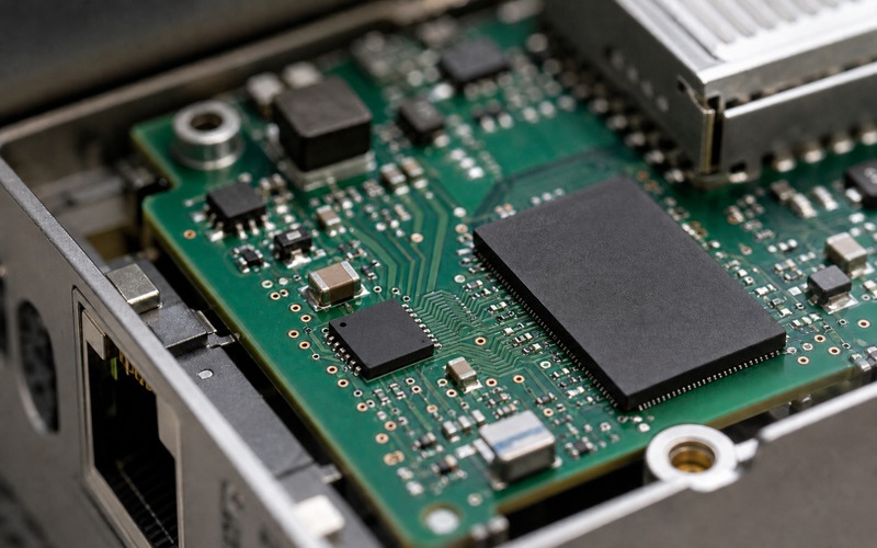
Confirm the Exact Device Before Reusing a Family Schematic
Start with the full W25Q64JVZEIM code and the current manufacturer page, package drawing and device documentation. The verified device is 64 Mb, which corresponds to an 8 MB nominal address space. Its operating supply is 2.7 to 3.6 V, the listed temperature range is -40 to +85 C, and the package is an eight-pad SON/WSON style. The family supports SPI, Dual SPI and Quad SPI. The published family rates reach 133 MHz for single-transfer-rate operation and 66 MHz for double-transfer-rate operation, subject to the selected mode and timing conditions.
A schematic copied from another density or suffix needs a deliberate review. Confirm pad numbering, supply pins, chip select, serial clock, bidirectional data pins, hold or reset behavior, write protection and the exposed-pad treatment shown in the exact package documents. Do not infer those details from a distributor thumbnail or from the top mark of a loose device. Record the document revision used for symbol and footprint release.
The orderable code also belongs in the bill of materials, approved manufacturer list, programming specification and receiving criteria. If another suffix is proposed, compare package, voltage, temperature, packing form and device behavior before treating it as the same material. A family name on the schematic is useful for readability; it is insufficient as the controlled purchasing identity.
Turn 64 Megabits Into a Real Capacity Budget
Sixty-four megabits equals eight megabytes of raw address space. The usable product budget must reserve space for the bootloader, primary firmware, configuration, calibration, certificates, file-system metadata and recovery records. If the product stores graphical assets, voice prompts, lookup tables or a compact model segment in serial flash, those items need measured sizes rather than early estimates. Erase alignment and update metadata can consume additional space around each region.
An A/B update design can be tight in 8 MB because two independently bootable images, a recovery component and persistent data must coexist. Build a partition table from the largest credible signed image, then add growth margin based on features already planned. Compression can reduce transfer size, but the processor still needs enough execution or staging space and a safe failure path. A design that fits only the current build has no room for a security patch or changed certificate chain.
Keep volatile working memory separate from this calculation. Serial NOR can hold executable code, constants and retained records, but it does not replace the bandwidth and write behavior of SRAM or DRAM. If an AI workload copies weights or kernels from flash into working memory, boot time depends on the transfer mode, controller efficiency, verification step and decompression work as well as the flash clock rate.
Choose the Read Mode the Processor Can Actually Boot
The device family offers ordinary serial, dual and quad transfers, yet the processor boot ROM may support only a subset. Confirm the boot source mode, opcode sequence, address width, dummy cycles and data-line behavior in the processor documentation. A fast quad read selected by application firmware is irrelevant if the immutable boot ROM starts in a simpler mode or expects different configuration bits.
Treat 133 MHz STR and 66 MHz DTR as device capability boundaries, not as guaranteed board settings. The usable rate depends on controller timing, voltage, temperature, trace delay, loading, input thresholds and the exact read command. Begin initial bring-up at a conservative clock, read identification and known data repeatedly, then increase speed while checking the full operating range. Save the chosen mode and timing register settings with the released firmware.
Execute-in-place can reduce copying at startup, but random access over serial flash has latency and bus-contention consequences. Measure the actual instruction and data pattern, cache behavior and interrupt response. Systems with deterministic startup needs may authenticate and copy selected regions into faster memory instead. The right choice follows measured boot and runtime behavior, not the highest number on a product table.
Design the 3 V Supply for Startup and Write Events
The 2.7 to 3.6 V range must be met at the flash pins during power ramp, read bursts, programming and erase operations. Place a small ceramic bypass capacitor close to the supply and ground pads, with a short return path. Check the regulator sequence shared with the processor and any level translator. If the processor drives signal pins before flash power is valid, leakage through protection structures can create partial powering and an unreliable reset state.
Power loss during a program or erase operation can leave the target region incomplete. Hardware should provide a clean reset and a voltage monitor or supervisor strategy appropriate to the product. Firmware should update data through versioned records, checksums and commit markers so that an interrupted write does not destroy the last known-good state. Critical configuration deserves redundant storage or another recovery method.
Measure the rail on the assembled board instead of relying only on the regulator label. Probe at the flash decoupling point while the processor boots and while representative program and erase work is running. Review ramp monotonicity, minimum voltage, ripple and shutdown behavior. Brownout testing should include repeated cycles near the threshold, because a single normal power cycle rarely exposes marginal sequencing.
Place the WSON-8 Package for Short and Inspectable Routing
The leadless eight-pad package saves board area, but the footprint requires the exact mechanical drawing. Verify body size, pad pitch, terminal length, pin-one indicator and any exposed center-pad requirement before releasing the land pattern. The package designation alone is not enough because other vendors and other family members may use different body dimensions or center-pad guidance while sharing an eight-contact description.
Place the flash close to the processor or controller that owns the bus. Keep clock, chip select and data lines short over a continuous reference plane. Avoid stubs, plane splits and unnecessary vias. Route the clock with particular care because its edge rate, rather than the nominal frequency alone, drives ringing and crosstalk. If optional series damping is provided, place it near the driver and validate the fitted value on hardware.
Keep programming access practical without creating long branches on the active bus. A compact test-point group, a controlled isolation option or a connector at the board boundary can support recovery and manufacturing. Any external connector must face the enclosure or board edge where a tool can mate without crossing the populated board. Document whether the processor must be held in reset or disconnected while an external programmer drives the flash.
Control Paste, Reflow and Side-Fillet Inspection
A WSON device has no gull-wing leads that make every joint obvious. The stencil opening, paste volume, solder-mask definition, surface finish and reflow profile need to suit the manufacturer's land recommendation and the assembly process. Excess paste under a center area can float the package or create voiding, while too little paste on perimeter pads can produce weak or open joints. Keep the package flat and the pin-one orientation visible through assembly documentation.
Side fillets can provide useful evidence when the terminal geometry exposes them, but visual inspection cannot prove every hidden interface. Use magnification and X-ray according to risk, especially during first-article assembly or after a process change. Compare suspect boards with a known-good image. An intermittent data line can resemble a timing or firmware fault, so assembly evidence should be reviewed before changing protocol settings to mask the symptom.
Include the flash in boundary or functional tests that exercise every data line. A simple identification read may pass even when a quad data connection is open because the first command uses one data line. The test should enter the intended transfer mode, write a pattern across representative addresses, verify it, power-cycle the board and read it again. This connects solder quality to the real operating interface.
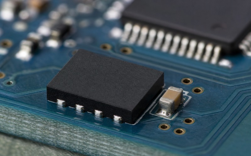
Bring Up Identification, Status and Protection Deliberately
At first power, read the manufacturer and device identification through the same controller instance used by the product. Record the response and compare it with the accepted list. Where Serial Flash Discoverable Parameters are used, parse them defensively and retain a known configuration for the exact part. A driver should reject an unknown identity or fall back to a safe diagnostic state rather than applying erase commands based on a guessed geometry.
Review status-register fields, write-enable behavior, busy polling, block protection, quad-enable control, reset commands and power-down recovery in the exact documentation. These details often differ across device generations or vendors even when standard read opcodes look familiar. The bootloader and application must agree about which code owns configuration changes and which bits are preserved.
Test the recovery path with protection enabled, after an interrupted operation and after a watchdog reset. Verify that the system cannot erase the active boot region through an ordinary configuration update. If factory programming changes security or one-time settings, make those actions explicit, auditable and separated from routine image programming.
Define Erase and Program Behavior in the Storage Layer
Serial NOR changes data through program and erase operations with alignment and one-way bit-transition constraints between erases. The storage layer should hide those rules from higher-level application code. Define region ownership, erase units, program chunks, timeouts, retries and error reporting from the exact device documentation. Never let two software components update the same region without a shared transaction model.
Persistent records benefit from sequence numbers, length fields, checksums and a final validity marker. Write new data into an erased location, verify it, then commit it before reclaiming the old copy. Wear should be distributed for frequently changing counters or logs. A device health strategy can track operation failures and retire a region before a latent problem reaches the boot record.
Concurrency matters when code is executed from the same flash being modified. Confirm whether the controller or processor can read while a program or erase command is active and how interrupts are handled. Critical routines may need to run from RAM, and the update service may need to suspend tasks that fetch from flash. Test this behavior under the real scheduler rather than in an isolated programming utility.
Build a Recoverable Firmware Update Layout
A reliable update begins with immutable or strongly protected first-stage code that can verify candidate images and choose a known-good path. The layout should retain enough information to distinguish empty, downloading, verified, active and rejected images. The product must recover after power removal at each transition. Exercise those transitions with repeated fault injection instead of testing only a complete update.
Cryptographic signatures protect image authenticity, while version and rollback policy protect the intended release state. Store public keys, counters and device-specific records in regions whose write authority is clear. One-time programmable features can support identity or policy, but their exact behavior must be confirmed before use because a mistaken permanent write cannot be repaired through normal software.
Service access needs the same discipline. Decide whether a board can be recovered through processor ROM, a debug connection or direct flash programming. Protect the route in the finished product while keeping a controlled manufacturing and repair method. Record which image, key set, programmer setting and verification hash were used on each released build.
Verify Production Programming Beyond a Successful Write
The production file should specify image version, address map, fill policy, protected regions and the expected final hash. Programming equipment needs an approved device algorithm for the exact flash. After programming, read back or independently verify the programmed range rather than accepting a tool's completion message alone. Confirm blank areas and configuration registers when they affect boot behavior.
Run a power-cycle boot after programming and test the intended quad or dual mode in addition to the basic serial identification path. Link the result to the board serial number and software release. If programming occurs before assembly, maintain component identity and moisture controls through placement. If it occurs in circuit, verify that other bus devices and processor pins cannot contend with the programmer.
A first-article run should include timing margin, low-voltage startup and representative temperature testing. Production screening can then focus on checks that reliably detect assembly and programming defects. Keep a known-good programmed board and captured bus traces as references for later process changes or supplier investigations.
Qualify Replacements at Hardware and Command Level
A proposed replacement must match more than 64 Mb and a 3 V supply. Compare package dimensions, pad map, center pad, voltage range, temperature grade, input thresholds, maximum clock modes, power behavior and reset response. Verify that the alternate device can be assembled with the released stencil and inspected by the current process.
At software level, compare identification, parameter discovery, read commands, dummy cycles, quad-enable handling, status and protection bits, reset sequence, suspend behavior, program limits, erase commands and error reporting. Avoid a driver that accepts any 64-megabit identity while assuming one vendor's register map. Use a device table with explicit capabilities and tested initialization paths.
Run the complete boot, update, power-fault and recovery suite on each approved source. Capture the exact code and document revision used. A pin-compatible device that boots at room temperature can still fail during a protected update, at a voltage corner or after a reset in the middle of erase activity. Approval should reflect the product use case, not a short bench demonstration.
Review Lifecycle Evidence Without Changing the Circuit Blindly
Before design release, confirm the exact orderable code, manufacturer lifecycle indication and change-notification path. Keep the approved source record tied to the full suffix. If the device later requires a second source, begin qualification while the original hardware and firmware references are available. This allows controlled comparison instead of a rushed substitution after a purchasing event.
Changes in package assembly, die revision or test location deserve engineering review when they affect the evidence used in qualification. Review manufacturer notices, update the affected documents and decide whether inspection, timing or reliability tests need repetition. Traceability is valuable because it connects a field observation to the material and process actually used.
Purchasing should request the exact approved code and reject silent suffix changes. Incoming inspection confirms label, package and order identity, while functional testing confirms the programmed system. These controls support each other; neither purchasing paperwork nor a boot test alone establishes equivalence.
Use a Final W25Q64JVZEIM Design Checklist
Confirm the 8 MB capacity budget, update layout and growth margin. Verify 2.7 to 3.6 V operation, decoupling, power sequencing and brownout recovery. Confirm processor boot-ROM commands, selected serial or quad mode, clock margin and execute-in-place behavior. Release the exact WSON-8 land pattern, stencil, orientation and inspection plan.
Check identification, parameter handling, status bits, protection, reset, erase, program and recovery in the released driver. Program and read back the production image, then power-cycle and boot through the intended interface. Preserve controlled service access and protect active boot regions. Run fault injection at update transitions and retain the logs with the software release.
For every approved alternate, repeat hardware, command and recovery comparisons with the full orderable code. Keep product, package and lifecycle evidence current. This checklist turns a small serial flash into a controlled boot subsystem whose capacity, electrical behavior, assembly and software remain aligned from prototype through production.
Related information
- 2026.07.14 MX25V1006FZUI as a Small Density SPI Flash
- 2026.07.14 W25N01GVZEIG as a 1 Gigabit SPI NAND Flash
- 2026.07.14 Planning Supply for a Ten Year AI Product


