 Free Shipping Over$200

- Products
- Marking
- Alternative

W25N01GVZEIG as a 1 Gigabit SPI NAND Flash
W25N01GVZEIG as a 1 Gigabit SPI NAND Flash
The W25N01GVZEIG is a 1-gigabit serial NAND flash device for products that need substantially more code or retained data than a small serial NOR can provide. The exact part operates from 2.7 to 3.6 V across -40 to +85 C, uses an 8 x 6 mm SON/WSON-8 package, supports SPI, Dual SPI and Quad SPI, and is specified for a 104 MHz single-transfer-rate clock. Its internal organization uses 2048-byte data pages with a 64-byte spare area, built-in 1-bit error correction, Buffer Read as the default mode and Continuous Read as an available option.
Those specifications describe a NAND device, not an oversized NOR device. A read begins by transferring a page from the array into an internal cache before data leaves through the serial interface. Programming loads the cache and then commits a page to the array. Erase operations act on blocks, some blocks may be marked bad from the factory, and bit errors must be interpreted through the device's correction status. A controller that simply increases an address range in an existing NOR driver will mishandle the memory.
A sound design review therefore covers the storage architecture, processor boot support, bad-block policy, ECC reporting, power-fail behavior, page and spare-area layout, production programming and replacement qualification. The goal is a repeatable storage subsystem whose data remains traceable from an image file to the programmed board and through field updates.
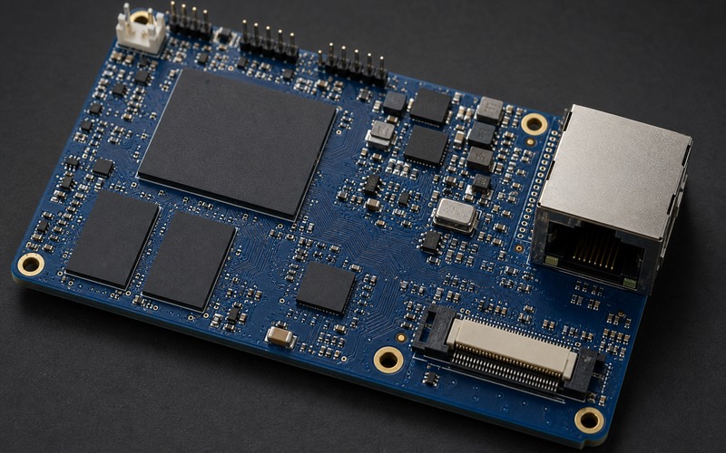
Confirm the Exact W25N01GVZEIG Configuration
Begin with the complete orderable code and current manufacturer information. W25N01GVZEIG is the 3 V, 1 Gb, industrial-temperature, 8 x 6 mm SON/WSON-8 configuration listed with SPI, Dual and Quad interfaces. Its 104 MHz rating is a device boundary for supported read operations; the released board setting must still satisfy controller timing, voltage, loading and command requirements. Keep the exact suffix in the bill of materials, approved source record, programming definition and incoming inspection criteria.
Verify pad numbering, chip select, clock, bidirectional data pins, write protection or reset behavior, supply and exposed-pad instructions from the exact package and device documents. An eight-contact body from another family can share an outline while using different pad behavior or thermal-pad guidance. Record the source and revision of the symbol and footprint evidence.
The one-gigabit density corresponds to 128 MB of raw binary capacity. That number is a starting point rather than the application-visible total. Factory bad blocks, runtime replacements, metadata, reserved recovery areas and file-system structures reduce the capacity available for images and user data. State the guaranteed application budget after those deductions instead of presenting 128 MB as a fully allocatable volume.
Decide Whether the Processor Can Boot From Serial NAND
Many processors advertise QSPI boot but implement a ROM sequence designed for serial NOR. Serial NAND requires a page-to-cache command, busy polling, a cache-read command and bad-block awareness before the requested bytes reach the processor. Confirm that the processor's immutable boot ROM names this device family or implements the required NAND sequence. A generic QSPI pin group does not prove boot compatibility.
If the ROM cannot manage NAND, use a supported first-stage source such as internal ROM, a small serial NOR, eMMC or another boot medium. That first stage can initialize the W25N01GVZEIG, read a verified image and copy it into RAM. The partition and recovery plan must then keep the first-stage dependency clear. A field update must never replace the only code capable of locating good NAND blocks.
When direct execution or continuous read is considered, verify how the processor handles page boundaries, cache refills, dummy cycles and error status. Measure instruction fetch behavior and interrupt latency with the intended cache and memory controller. Code shadowing into RAM is often easier to validate because the NAND path is exercised during a controlled load rather than on every random instruction fetch.
Design Around the 2048 Plus 64 Byte Page
The main data area is organized in 2048-byte pages with 64 spare bytes associated with each page. Software should use the exact page and block geometry from current device documentation rather than calculating it from density alone. Define where file-system metadata, logical-to-physical mapping data, error-correction information and bad-block markers live. The spare area is controlled storage, not a free extension of the user payload.
A page read first moves array data into the device cache. The controller waits for completion, checks status and then reads from the cache through the selected serial width. A program operation loads data into the cache before program execute commits it to the array. Splitting or repeating those stages incorrectly can return stale cache content, wrap within a page or corrupt a partially prepared page.
Align higher-level writes to page and erase-block boundaries where practical. Small records should be aggregated or managed by a NAND-aware file system so frequent updates do not force repeated block relocation. The application API should expose atomic records, checksums and commit states while the lower layer handles page placement and block reclamation.
Use On-Chip ECC Without Hiding Its Status
The exact product specification lists built-in 1-bit ECC. Enable and use it according to the device documentation, then read the correction result after each page transfer. A successful data read and a corrected-error indication are different maintenance events. The driver should distinguish clean data, corrected data, uncorrectable data and command failure, and should pass meaningful results to the storage health layer.
A corrected page may remain readable, yet it can signal that data should be refreshed into a known-good block before margin declines further. Define a scrub or relocation policy for persistent records and firmware images. Uncorrectable data needs a recovery source, a redundant copy or a controlled failure state. Repeated blind retries can return the same failing page without protecting system integrity.
Do not combine an external software ECC layout with the internal mechanism until the ownership of every spare byte is documented. Boot code, production tools and the field driver must use the same ECC and spare-area policy. Otherwise an image programmed successfully by one tool may appear damaged to another implementation that interprets the extra bytes differently.
Preserve Factory Bad-Block Information
NAND flash can contain factory-marked bad blocks, and additional blocks can become unsuitable during use. The receiving and programming process must preserve the manufacturer's bad-block markers. Do not mass-erase a fresh device or overwrite spare bytes before the programmer has scanned and recorded those markers. An image writer should skip bad blocks and continue according to one documented logical mapping method.
The W25N-GV family provides a bad-block-management lookup capability that can map defective blocks to reserved good blocks. Confirm the exact commands, table capacity, update rules and power-fail behavior before relying on it. The host may instead maintain its own logical map or use a NAND-aware file system. Mixing two independent remapping policies without a clear boundary makes diagnosis difficult.
Reserve enough good blocks for replacement, metadata copies and recovery images. Capacity planning should use the minimum usable result required by the product, not the best result from one sample. During field operation, record when a block is retired and protect the mapping update with redundant metadata and sequence numbers.
Select Buffer or Continuous Read Deliberately
W25N01GVZEIG defaults to Buffer Read and offers Continuous Read as an option. Buffer Read keeps page transfer and cache access explicit, which makes status and page boundaries easier to control. Continuous Read can improve a sequential workload, but the controller and driver must agree on entry, exit, boundary behavior and recovery after reset. Save the chosen mode as part of the released configuration.
The 104 MHz device rate does not directly equal application throughput. Array-to-cache latency, command overhead, busy polling, serial width, controller efficiency and software copies all contribute. Benchmark the complete path with realistic image sizes and access patterns. A video recorder, network appliance and boot loader stress the same flash in different ways.
Start signal-integrity work at a conservative clock. Verify identification, cache reads and full-page patterns, then increase the rate across voltage and temperature. Inspect clock, chip select and data timing at the flash pins. Edge quality, return-path continuity and pin loading can limit a board even when the nominal frequency is below the published maximum.
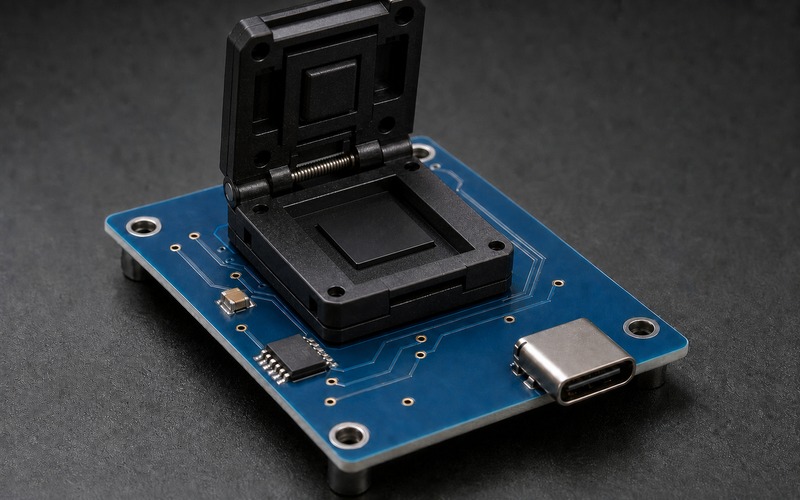
Lay Out and Assemble the WSON-8 Package Correctly
Use the exact 8 x 6 mm SON/WSON drawing for body dimensions, terminal geometry, pin-one orientation and exposed-pad treatment. Place the flash near the owning controller with short clock, chip-select and data traces over a continuous reference plane. Keep optional damping close to the driver. Avoid stubs from test points and prevent a service connector from extending the active bus deep across the board.
Board-edge connectors must face the enclosure opening or the outside of the PCB so a cable or programmer can mate without crossing populated components. When an external programmer shares the bus, define how the processor is held in reset or isolated. Power from the programmer must not back-feed the product rail or partially power the controller through signal pins.
The leadless package needs a controlled stencil, paste volume, reflow profile and inspection method. Side evidence may be limited, so first-article builds can require magnification and X-ray. Exercise every serial data line after assembly. A basic single-line identification command can pass while a quad connection remains open.
Protect Writes Against Power Loss
Programming and block erase take place after commands have been accepted, so power removal can interrupt an operation after the host has moved on to other work. Monitor device busy and failure status, keep the rail within specification, and use a reset or supervisor strategy matched to the system. Test the voltage at the flash during page programming and block erase, not solely during idle boot.
Persistent metadata should use at least two recoverable copies with generation counters, checksums and final validity markers. Write a new copy into prepared space, verify it, then commit it before reclaiming the old version. The logical block map and firmware activation record deserve this treatment because losing either can make all otherwise valid pages unreachable.
Inject power failures at every update stage: page load, program execute, mapping update, image verification, activation and old-block reclamation. On restart, the system should choose the last complete state and quarantine uncertain pages or blocks. A clean update performed once on a bench does not test this recovery path.
Choose a NAND-Aware Data and Firmware Layout
Separate immutable recovery code, signed firmware images, frequently changing configuration and bulk event data. Each class has different redundancy, update and wear requirements. Store image headers and hashes where the loader can find them even after a block is retired. A logical partition table must be translated through the selected bad-block policy rather than assuming fixed physical addresses forever.
For file storage, use a file system or translation layer designed for raw NAND behavior. It should manage erase units, page writes, wear distribution, garbage collection and interrupted operations. A simple NOR-style key-value store that rewrites fixed addresses can consume blocks unevenly and lose records during relocation.
Keep enough RAM for page buffers, verification and decompression. A 2048-byte page is small compared with an image, but multiple buffers may be needed to pipeline reads or preserve metadata during an update. Measure the complete boot path from array transfer through authentication and copy into working memory.
Program Production Units With Bad-Block Awareness
The production definition should include image version, logical layout, page and spare-area policy, ECC configuration, bad-block method and final verification hashes. Use a programmer algorithm approved for the exact device. Before writing, read identification and factory markers. During programming, skip or remap bad blocks without destroying their evidence.
Verification should read the logical image back through the same ECC and mapping assumptions used by the product. A raw byte comparison can fail for acceptable corrected data or pass while ignoring an incorrect logical map, depending on the tool. Record programmed device identity, image hash, tool version and board serial number so a later failure can be reproduced.
After programming, remove power and boot through the intended product path. Read representative pages in the selected serial mode, review ECC status and test recovery metadata. If devices are programmed before assembly, preserve their identity through handling. If programming occurs on the board, prevent bus contention and validate the outward-facing service connection.
Qualify Replacements Beyond Density and Pinout
A candidate replacement must match supply, temperature, package dimensions, pad map, center pad, clock modes and power behavior. A similar 1 Gb part may operate at 1.8 V, use a different default read mode, require stronger ECC or assign spare bytes differently. These differences can invalidate both the board and stored-image format even when the package fits.
Compare identification, page geometry, block geometry, cache commands, status fields, ECC reporting, bad-block markers, remapping features, reset, protection and power-down behavior. The driver should select an explicit capability record from the verified identity instead of accepting every device with the same density.
Run boot, sequential read, random page access, page program, block erase, corrected-error handling, bad-block skip, power-fail update and recovery tests on every approved source. Preserve the exact suffix and documentation revision in the approval. A short room-temperature read test is insufficient evidence for a storage substitution.
Use a Final SPI NAND Design Checklist
Confirm the exact W25N01GVZEIG identity, 2.7 to 3.6 V rail, -40 to +85 C range, 8 x 6 mm WSON-8 footprint and 104 MHz timing plan. Verify that the processor boot path understands serial NAND page-to-cache behavior. Define the 2048+64-byte layout, internal ECC policy, bad-block markers, remapping ownership and guaranteed usable capacity.
Release the Buffer or Continuous Read configuration, signal-integrity margin, decoupling, power-fail strategy and WSON assembly inspection. Test all data lines, status outcomes and recovery states. Program through a device-specific path, preserve factory markers, read the logical image back and perform a cold boot with the released software.
For each alternate, repeat electrical, package, command, ECC, page-layout and bad-block comparisons. Keep the image format, programmer setup and runtime driver synchronized. These controls turn the 1-gigabit device into a dependable storage subsystem rather than a large but opaque memory component.
Related information
- 2026.07.14 MX25V1006FZUI as a Small Density SPI Flash
- 2026.07.14 W25Q64JVZEIM as a 64 Megabit SPI NOR Flash
- 2026.07.14 Planning Supply for a Ten Year AI Product


