Free Shipping Over$200

- Products
- Marking
- Alternative

The Cost of Moving From a Module Prototype to a Bare Chip
The Cost of Moving From a Module Prototype to a Bare Chip
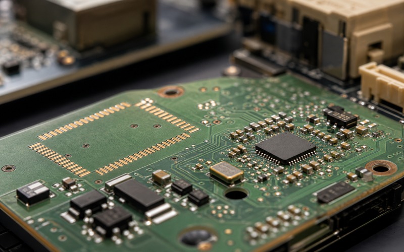
A module can make an early product feel almost finished. The processor, memory, radio, oscillator, power filtering, antenna matching and regulatory paperwork may arrive on one small board, and the first firmware team can start without owning every detail under the shield can.
The cost appears later, when the same product is expected to ship in volume with a bare IC on the main PCB. The module price is easy to see. The engineering work hidden inside the module is less visible until it has to be rebuilt, tested and supported by the product team.
The right question is not whether a bare-chip design is cheaper. It is whether the product can absorb the work that the module vendor used to carry: layout margin, RF tuning, power behavior, clock stability, boot storage, firmware bring-up, factory test, approvals, second sourcing and failure analysis.
Start With What the Module Was Doing
A module is rarely just a chip on a carrier. It often includes memory, flash, a crystal or oscillator, local regulators, RF matching, antenna feed, ESD parts, shielding, certification evidence, production test coverage and layout decisions that have already been debugged. Removing the module means taking those decisions back into the product design.
List the module functions before discussing cost. Which rails does it create locally? Which clock source does it use? Does it include configuration memory? Does the antenna path sit on the module, on the product board or partly on both? Which boot pins, strapping resistors and reset timing are already handled inside the module?
The list should also include non-electrical work. A module may carry documentation, radio reports, thermal guidance, firmware examples, production test recommendations and a known assembly process. Those items may not appear on the schematic, but they reduce risk during the prototype stage.
Once the module job is visible, the bare-chip project becomes a transfer plan rather than a blind cost-reduction step.
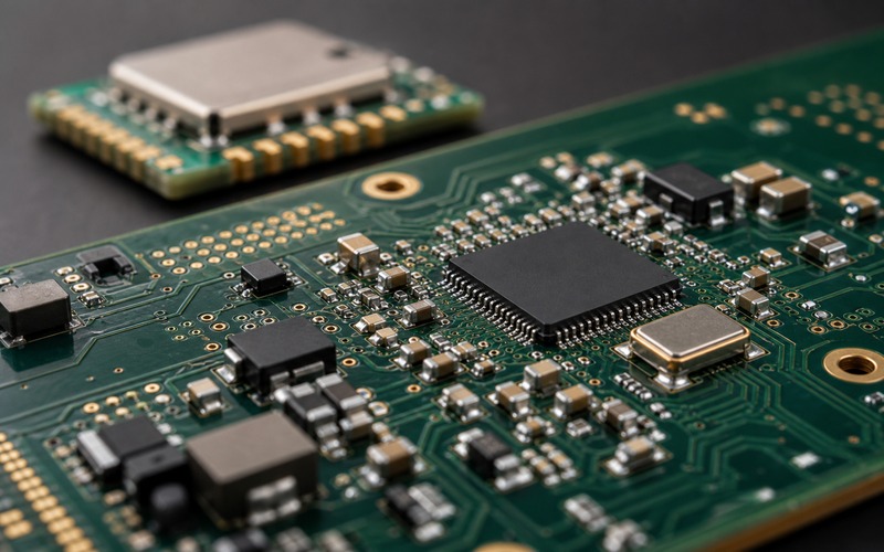
The Bare IC Pushes Layout Work Back Onto the Board
The first visible change is footprint and routing. A module may use large edge pads or a compact castellated outline that is forgiving to place and inspect. A bare IC may use QFN, BGA, LGA, WLCSP or another package that asks for tighter solder rules, more escape routing, shorter decoupling loops and a different board stackup.
Package choice drives cost in several directions. Fine pitch can raise PCB fabrication requirements. A thermal pad can demand via-in-pad or a controlled copper pattern. A BGA can require X-ray inspection. A WLCSP can reduce area while raising assembly sensitivity. These are not abstract manufacturing concerns. They change supplier choice, inspection method, yield learning and rework strategy.
Decoupling also moves from a module vendor's proven placement to the product board. Capacitor value, case size, dielectric, bias behavior and loop area all affect rail noise. The clock part and boot memory now need clean routing and stable power. Reset and strap pins need real production defaults rather than jumper-friendly prototype assumptions.
A bare-chip design may still be the right choice, but its layout cost is paid in board rules, review cycles and pilot builds. The savings per unit should be compared with that work, not with the chip price alone.
Power and Thermal Margins Need Fresh Proof
A module often hides its local power details. It may include regulators or at least local filtering chosen around the processor, radio or memory. Moving to a bare IC makes the main board responsible for load steps, ripple, sequencing, brownout behavior and heat flow.
The power tree should be redrawn from the input connector to the silicon pins. Check which rails must start first, which pins tolerate back-powering, what the peak current looks like during boot, radio transmit, memory access or inference, and how the regulator responds to those events. A rail that looks acceptable at average load can fail during a short burst.
Thermal behavior changes in the same way. The module may have a shield, copper area, carrier board and approved mounting guidance. A bare IC relies on the product PCB, vias, copper pours, enclosure contact and nearby heat sources. The board may save area and cost while losing the heat path that made the module stable.
Sustained performance, radio output, sleep current and reset behavior should be measured again on the bare-chip board. The earlier module result is useful background, but it is not proof for the new layout.
RF Designs Lose Their Borrowed Margin First
The penalty is sharpest when the module includes a radio. A certified module may arrive with a tuned RF path, shield, matching network, layout keepout and antenna recommendation. The product team can still harm the result with enclosure and antenna placement, but the highest-risk RF details are partly contained.
A bare radio IC puts those details on the product board. The feed line, matching parts, ground return, shield option, antenna transition, keepout, ESD location and nearby noisy circuits all become part of the design. A small component move can change output power, receiver sensitivity or compliance margin.
Certification planning changes as well. Some products can lean on a module's existing approvals when the antenna and use conditions match. A bare-chip radio path usually needs deeper RF validation and a broader approval plan. That can be acceptable in a high-volume product, but it belongs in the schedule before the first cost comparison is approved.
RF is not the only area affected, but it is the area where a small saving can turn into a lab delay. If the module was chosen to avoid RF risk, replacing it later needs a real RF budget, not a line item called layout cleanup.
Firmware Bring-Up Becomes a Board-Level Job
Module prototypes often start from a vendor image, sample project or board support package. The boot path, memory map, pin mux, clock tree, radio stack and low-power states may already match the module board. A bare-chip product board changes that support boundary.
Firmware work should be counted early. Boot configuration must match the selected flash or memory part. Pin assignments must match the final schematic, not the evaluation header. Power modes must account for every external pull, sensor, level shifter and regulator enable. Production update flow and secure boot choices may also change when storage moves from the module to the main board.
Debug access can shrink. A module dev board may expose serial, SWD, JTAG, boot pins and reset lines in friendly places. The product board may bury them behind pads or omit some access to save space. That decision affects bring-up, factory programming and field failure analysis.
A clean transition plan gives firmware a bring-up checklist tied to hardware revision. Without it, the bare-chip board can spend weeks proving that a problem is not the silicon, not the compiler, not the layout and not a missing strap.
Factory Test and Failure Analysis Must Be Rebuilt
A module may arrive tested as a small subsystem. The product line can test whether the assembled product sees the module, loads firmware and talks through the expected interfaces. Once the bare IC is placed directly on the main PCB, the factory test has to catch assembly, power, clock, boot, memory, RF and communication faults at board level.
Add test access while the layout is still flexible. Bring out key rails, reset, boot mode, debug, programming, RF checkpoints where relevant and enough functional signals to separate a solder fault from a firmware fault. Test pads cost board area, but missing test access costs time on every yield excursion.
Inspection strategy also changes. A castellated module may be visually inspectable. A BGA or fine-pitch IC may need X-ray, solder-process control, stencil adjustment and first-article review. Rework may become harder or less reliable, changing the economics of scrap versus repair.
Failure analysis should be discussed with manufacturing before volume. If a field return arrives, can the team tell whether it is firmware, solder, ESD, power stress, RF detuning or memory corruption? The module used to narrow that search. The bare-chip design has to recreate that diagnostic path.
Sourcing Risk Moves From One Line Item to Many
A module concentrates sourcing into one approved part number, often with a single supplier and a known firmware support path. A bare-chip design spreads the approved set across the main IC, memory, oscillator, RF parts, passives, regulators, shield, antenna, package process and test fixtures.
This can improve control. The buyer can second-source passives, choose the memory grade, manage lifecycle by component and negotiate at a lower level. It can also increase exposure. A small oscillator shortage, flash revision change or RF matching part substitution can stop a board that used to buy one module line.
The approved vendor list should be built with engineering, purchasing and manufacturing together. Pin-compatible or value-compatible substitutes are not enough when timing, RF, thermal or boot behavior depends on the exact part. Each substitute needs a validation rule tied to the circuit function.
The cost model should include this work. Unit savings from a bare IC are strongest when volume is high, the design life is long and the team can maintain the component set. At lower volume, the module may still be cheaper after engineering time, approval cost and supply risk are counted.
Cost Comparison Needs a Real Boundary
A useful cost comparison has three columns: module path, bare-chip path and one-time work. The module path includes module price, module supply risk, board area, connector or antenna constraints and dependency on module firmware support. The bare-chip path includes IC price, added components, PCB rules, assembly steps, inspection, test, certification and engineering hours.
One-time work is where weak decisions hide. Schematic redesign, layout, RF tuning, power validation, thermal test, firmware port, factory fixture update, documentation, compliance work and pilot yield learning should be visible. If those items are ignored, the bare-chip design will look better than it is.
The boundary should match the business goal. A short-life, low-volume product may value speed and reduced risk. A high-volume product may earn back the redesign. A regulated or wireless product may need approval cost placed near the center of the decision. A product with uncertain demand may keep the module for the first release and design the board so a later bare-chip revision is possible.
The decision is sound when both paths are priced against the same release condition: product performance, test coverage, approval status, support plan and supply risk.
Transition Checklist
Before replacing a prototype module with a bare IC, review module functions, package choice, PCB stackup, decoupling, power sequencing, clocking, memory, RF path, antenna, firmware bring-up, programming access, factory test, inspection, certification and approved alternatives.
Move to the bare chip when the unit savings, control and supply strategy justify the engineering work. Keep the module when speed, approval reuse, RF containment or low-volume economics matter more than the component price delta.
Related information
- 2026.07.10 How Lens Distortion Bites a Vision Model