- Products
- Marking
- Alternative
Texas Instruments 1P1G14MDBVREP

- Part No.:
- 1P1G14MDBVREP
- Manufacturer:
- Texas Instruments
- Category:
- Gates and Inverters
- Package:
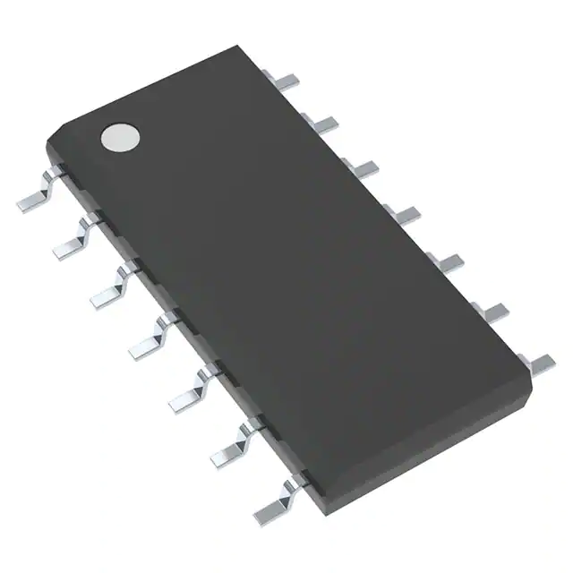
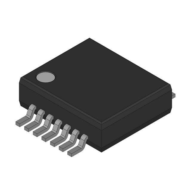
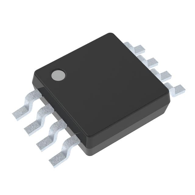
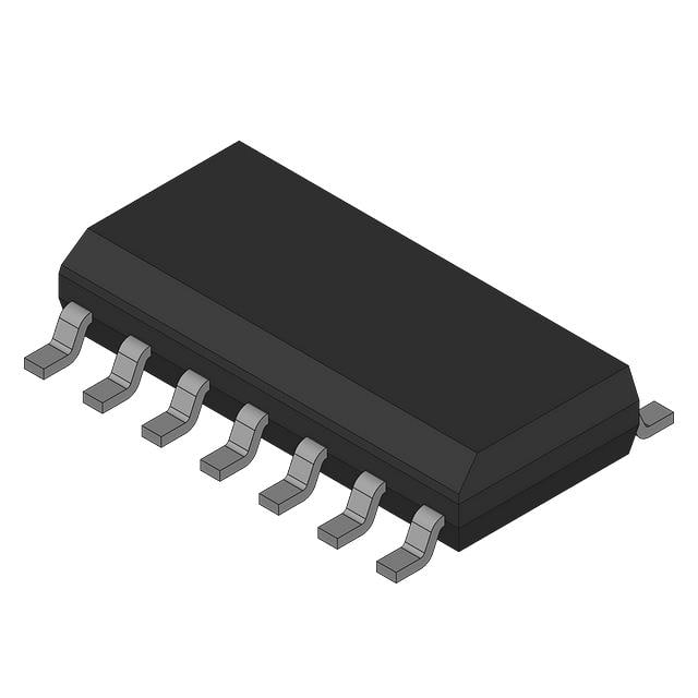
- SC-74A, SOT-753
- Datasheet:
-
 1P1G14MDBVREP.pdf
- Description:
- IC INVERTER 1CH 1-INP SOT23-5
- Quantity:
Unit Price:$0.000000
Ext Price:$0.000000
- Payment:

- Shipping:

Inventory:0
Send us your inquiry,we will respond immediately.
In Stock : 0 PCS
| Qty. | Unit Price | Ext Price |
| 0+ | $0.000000 | $0.000000 |
*Products eligible for online ordering ship within 1-2 business days,please contact us for exact shipping times.
Also you can RFQ for 1P1G14MDBVREP or email to us: Email: [email protected] , we will contact you within 12 hours.
Product Details
1P1G14MDBVREP (Texas Instruments SN74LVC1G14-EP) - Enhanced-Product Single Schmitt-Trigger Inverter, SOT-23-5
1P1G14MDBVREP is the InFortune ordering code for the Texas Instruments SN74LVC1G14-EP, a single Schmitt-trigger inverter built to TI’s Enhanced-Product (EP) programme (controlled baseline, extended −55 °C to +125 °C). Its true input hysteresis turns slow, noisy or rounded edges into one clean, fast logic transition (Y = NOT A). It runs on 1.65 V to 5.5 V, has 5.5 V-tolerant inputs, drives ±24 mA at 3.3 V, supports Ioff, and ships in a 5-pin SOT-23 (DBV).
Product Introduction
The SN74LVC1G14-EP is a single-gate Schmitt-trigger inverter: it inverts its input (Y = NOT A), but unlike an ordinary inverter it has a true Schmitt-trigger input with separate positive-going (VT+) and negative-going (VT−) thresholds. That hysteresis — roughly 0.56 V wide at 3.3 V — means a slow, noisy or ringing signal still produces exactly one clean, fast output edge instead of multiple glitches.
That makes it the standard tool for signal conditioning: squaring up the output of an RC delay, cleaning a slow sensor or switch edge, restoring a degraded clock, or providing noise immunity at the input of a logic chain. Because it is a single gate in SOT-23, it does that job exactly where the noisy signal enters the board.
This order option is the “-EP” Enhanced Product: a controlled baseline (one fab, one assembly/test site), DMS support, change notification and an extended −55 °C to +125 °C grade. Electrically it is a full LVC gate — 1.65 V–5.5 V, 5.5 V-tolerant inputs, ±24 mA drive, Ioff partial-power-down — for harsh, long-life equipment that must keep cleaning its signals over temperature.
Expert Technical Insight
Getting the most from a Schmitt-trigger inverter:
- Hysteresis is the whole point: the gap between VT+ and VT− (about 0.56 V at 3.3 V) sets how much noise the input rejects. A signal must cross VT+ to flip the output one way and fall below VT− to flip it back, so noise smaller than the hysteresis band cannot cause a false transition.
- It tolerates arbitrarily slow edges: unlike a plain inverter (or the “Schmitt-action” AHC1G04), a true Schmitt-trigger has no upper limit on input rise/fall time — ideal for RC ramps and slow sensor lines.
- The EP grade keeps it honest over temperature: the −55 °C to +125 °C controlled-baseline qualification means the thresholds and timing stay within spec in harsh, long-deployment equipment, not just at room temperature.
Key Benefits
Separate VT+/VT− thresholds (~0.56 V at 3.3 V) reject noise and square up slow or ringing edges into one clean transition.
Controlled baseline, DMS support and extended temperature for long-life, harsh-environment equipment.
LVC supply range with 5.5 V-tolerant inputs and strong drive for mixed-rail signal conditioning.
Output disables when unpowered, preventing back-current into a still-live downstream node.
Specifications
| Parameter | Value | Conditions / Notes |
|---|---|---|
| Device Type | Single Schmitt-trigger inverter (Enhanced Product) | One channel; LVC family |
| Manufacturer | Texas Instruments | SN74LVC1G14-EP (data sheet SCES674) |
| Logic Function | Y = NOT A | True Schmitt-trigger input |
| EP Grade | Controlled baseline; M-temp | DMS support; change notification |
| Input Hysteresis (VT+ − VT−) | ≈ 0.56 V typ at 3.3 V | VT+ ≈ 1.5 V, VT− ≈ 0.84 V (at 3 V) |
| Supply Voltage (VCC) | 1.65 V to 5.5 V | Data retention down to 1.5 V |
| Input Tolerance | Up to 5.5 V | Input accepts voltages above VCC |
| Output Drive (IOH/IOL) | ±24 mA at 3.3 V | ±32 mA at 4.5 V |
| Propagation Delay (tpd) | 4.6 ns max at 3.3 V | CL = 15 pF; ~4.4 ns at 5 V |
| Ioff (partial power down) | ±10 µA max | VI/VO = 5.5 V, VCC = 0 |
| Quiescent Current (ICC) | 10 µA max | Up to ~19 µA over full M-temp range |
| Input Capacitance (Ci) | 4.5 pF typ | VCC = 3.3 V |
| ESD (HBM / MM / CDM) | 2000 V / 200 V / 1000 V | Exceeds JESD22 |
| Operating Temperature (TA) | −55 °C to +125 °C | M-temp (EP) |
| Package | 5-pin SOT-23 (DBV) | Order code SN74LVC1G14MDBVREP |
Note: Values are from the Texas Instruments SN74LVC1G14-EP data sheet (SCES674). Confirm every parameter, especially the temperature-dependent thresholds and timing, against the latest data sheet before committing a design.
Package Information
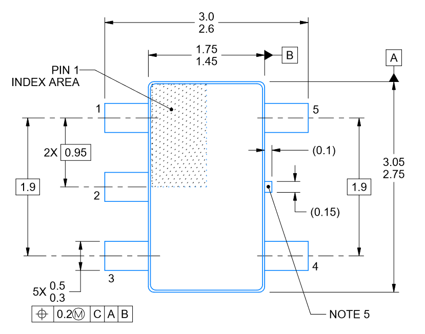
The SN74LVC1G14-EP in this order option (MDBVREP) ships in the DBV 5-pin SOT-23 (JEDEC MO-178, 1.45 mm maximum height, body about 2.9 mm × 1.6 mm). The robust SOT-23 outline suits the harsh-environment boards the EP grade targets, where leads are easier to inspect and rework than a leadless package. Supplied tape-and-reel.
The dimensioned drawing below gives the SOT-23-5 body and lead geometry for the land pattern and assembly stencil.
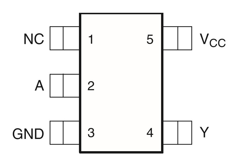
Pin Configuration (SOT-23-5)
The single inverter maps onto five pins (top view):
- Pin 1 – NC: No internal connection; leave open or tie to a plane for support.
- Pin 2 – A (Input): Schmitt-trigger logic input; 5.5 V-tolerant; accepts slow/noisy edges.
- Pin 3 – GND: Ground (0 V) reference.
- Pin 4 – Y (Output): Inverted output, Y = NOT A; drives ±24 mA at 3.3 V.
- Pin 5 – VCC: Supply, 1.65 V to 5.5 V; decouple with a local 0.1 µF capacitor.
Alternative Parts
The closest relatives are other single Schmitt-trigger gates. The SN74LVC1G17 is the non-inverting Schmitt-trigger (Y = A) counterpart; use it when you need clean-up without inversion. Confirm inverting vs non-inverting and the temperature grade before substituting.
| Part Number | Brand | Function | Package | Note |
|---|---|---|---|---|
| 1P1G14MDBVREPG4 | Texas Instruments | Schmitt inverter (EP) | SOT-23-5 | Same device, Pb-free (G4) ordering |
| SN74LVC1G17MDBVREP | Texas Instruments | Schmitt buffer (non-inverting), EP | SOT-23-5 | Non-inverting Schmitt counterpart, same EP grade |
| SN74LVC1G17DBVRG4 | Texas Instruments | Schmitt buffer (non-inverting) | SOT-23-5 | Commercial-grade LVC Schmitt buffer |
| SN74AUP1G17DBVRG4 | Texas Instruments | Schmitt buffer (non-inverting) | SOT-23-5 | Ultra-low-power AUP family |
Logic Family Comparison
| Family | Supply Range | Position | Use When |
|---|---|---|---|
| LVC-EP (this part) | 1.65–5.5 V | Wide-supply, 5 V-tolerant, −55/+125 °C | Harsh-environment signal conditioning |
| AHC | 2–5.5 V | General-purpose (Schmitt-action) | Basic 5 V/3.3 V clean-up |
| AUP | 0.8–3.6 V | Ultra-low-power | Battery / portable |
| AUC | 0.8–2.7 V | Very high speed | Sub-2 V core logic |
Manufacturer Information
Texas Instruments (TI, NASDAQ: TXN), of Dallas, Texas, is a leading logic supplier; its LVC Schmitt-trigger single gates (inverting '14 and non-inverting '17) are standard tools for signal conditioning, and the Enhanced-Product (EP) variants add an extended-temperature, controlled-baseline pedigree for long-life programmes.
The governing document is the SN74LVC1G14-EP data sheet (SCES674), which defines the Schmitt thresholds, the Ioff behaviour, the M-temperature timing and the DBV package. InFortune Electronics supplies the device under code 1P1G14MDBVREP and provides sourcing and technical support.
Application Areas


Frequently Asked Questions (FAQ)
What does the Schmitt-trigger input do?
It adds input hysteresis: separate positive- and negative-going thresholds (about 0.56 V apart at 3.3 V). A slow, noisy or ringing input therefore produces one clean, fast output transition instead of multiple glitches — ideal for conditioning real-world signals.
Is this a true Schmitt-trigger or just Schmitt-action?
A true Schmitt-trigger — it has no upper limit on input rise/fall time, so it handles arbitrarily slow ramps. (That is stronger than the “Schmitt-action” of a part like the SN74AHC1G04, which still limits edge slowness.)
What does the “-EP” designation add?
Enhanced Product: a controlled baseline (one fab, one assembly/test site), DMS support, change notification and an extended −55 °C to +125 °C qualification — for long-life, harsh-environment equipment.
Do you have a non-inverting version?
Yes — the SN74LVC1G17 is the non-inverting Schmitt-trigger buffer (Y = A); use it when you need the same edge clean-up without logical inversion.
Disclaimer
Information Accuracy: Technical specifications on this page are based on the Texas Instruments SN74LVC1G14-EP data sheet (SCES674). We strive for accuracy and completeness, but specifications are subject to change without notice.
Product Authenticity: We guarantee all products are genuine factory originals with complete material traceability.
Technical Support: Free technical consultation is available before and after purchase.
Application Note: This product page is for reference only. Suitability for a specific application should be verified by design engineers against actual system requirements.
1P1G14MDBVREP Specifications
- Specifications
- Attributes
- Property Value
- Manufacturer
- Texas Instruments
- Series:
- 74LVC
- Package/Case:
- SC-74A, SOT-753
- Packaging:
- Tape & Reel (TR)
- Part Status:
- Active
- Logic Type:
- Inverter
- Number of Circuits:
- 1
- Features:
- Schmitt Trigger
- Voltage - Supply:
- 1.65V ~ 5.5V
- Current - Quiescent (Max):
- 19 µA
- Current - Output High, Low:
- 32mA, 32mA
- Input Logic Level - Low:
- 0.39V ~ 1.87V
- Number of Inputs:
- 1
- Input Logic Level - High:
- 1.16V ~ 3.33V
- Max Propagation Delay @ V, Max CL:
- 5ns @ 5V, 50pF
- Supplier Device Package:
- SOT-23-5
- Operating Temperature:
- -55°C ~ 125°C
- Mounting Style:
- Surface Mount
- Grade:
- -
- Qualification:
- -
- Category:
- Gates and Inverters
1P1G14MDBVREP Relevant information
- 1P1G14MDBVREP Tags
- Popular Search
The following parts are popular search parts in Gates and Inverters.
The Posts
-
0473003.YRT1L LITTELFUSE Fuse: Applications, Selection Guide, Alternatives and Buying Notes
0473003.YRT1L LITTELFUSE guide for 3 A PICO II 473 slow-blow axial fuse use, 125 V ratings, alternatives and sourcing checks.

-
0451005.MR LITTELFUSE Fuse: Applications, Selection Guide, Alternatives and Buying Notes
0451005.MR LITTELFUSE fuse guide for 5 A NANO2 451 use, obsolete-status review, alternatives, replacement risk and sourcing checks.
-
0251.062NRT1L LITTELFUSE Fuse: Applications, Selection Guide, Alternatives and Buying Notes
0251.062NRT1L LITTELFUSE fuse guide for 62 mA PICO II 251 use, 125 V rating, axial PCB fit and sourcing checks.
-
0251001.NRT1L LITTELFUSE Fuse: Applications, Selection Guide, Alternatives and Buying Notes
0251001.NRT1L LITTELFUSE guide for 1 A PICO II 251 axial fuse use, 125 V ratings, PCB fit, alternatives and sourcing checks.
-
0154001.DR LITTELFUSE Fuse: Applications, Selection Guide, Alternatives and Buying Notes
0154001.DR LITTELFUSE fuse guide for 1 A OMNI-BLOK 154 use, 125 V rating, PCB footprint review, alternatives and sourcing checks.
-
0154.062DR LITTELFUSE Fuse: Applications, Selection Guide, Alternatives and Buying Notes
0154.062DR LITTELFUSE fuse guide covering 62 mA OMNI-BLOK use, 125 V ratings, PCB holder fit, alternatives and sourcing checks.
-
XH414HG-IV01E SEIKO EDLC: Applications, Selection Guide and Buying Notes
XH414HG-IV01E SEIKO EDLC guide for 3.3V RTC backup, IV01E pinout and terminal checks, alternatives, replacement risk and sourcing review for buyers before RFQ.
-
XH414HG-II06E SEIKO EDLC: Applications, Selection Guide and Buying Notes
XH414HG-II06E SEIKO EDLC guide covering RTC backup use, 3.3V charging, opposite-side pinout and terminals, alternatives, replacement risk and sourcing checks.
Related Products
-
74VHC86MX
Fairchild Semiconductor
-
74VHCT08AM
Fairchild Semiconductor

-
MM74HC02SJ
Fairchild Semiconductor
-
SN74ALS32DB
Texas Instruments
-
SN74ALS86NE4
Texas Instruments
-
74VHCT04AM
Fairchild Semiconductor

-
74HC21DB,112
NXP Semiconductors

-
NLVLCX08DTR2G
Cypress Semiconductor Corp
-
74LVX02M
Fairchild Semiconductor
-
74VHCT00AM
Fairchild Semiconductor
-
XC7WH14DP,125
NXP USA Inc.
-
74HCT4075D,652
Nexperia USA Inc.