Free Shipping Over$200

- Products
- Marking
- Alternative

Wiring Video Output and High Speed Lanes into an AI Device
An AI device often has to push a video signal out to a screen and move data across fast serial lanes inside itself, and both run at speeds where the copper stops behaving like a plain wire. Getting a display image off the processor and onto an HDMI monitor, or routing a PCIe link between two chips, is a job of bridges and switches and careful layout, not connecting pins. The parts that do it, and the board they sit on, decide whether the link runs clean or falls over.
The work splits in two. A signal that has to leave the device, the video to a display, often comes out of the processor in one format and has to be converted to the one the screen takes. A signal that stays inside, a high speed lane between chips, has to be routed, sometimes switched between destinations, and kept clean over its run on the board. Both are governed by the same fact, that at these data rates the connection is a transmission line and has to be treated as one.
Two kinds of high speed, out and across
Video output is a one way, high bandwidth stream from the processor to a screen, and the processor rarely speaks the screen's language directly. Many processors drive a display over MIPI DSI, a short reach interface meant for a panel wired close, while a monitor or a capture card wants HDMI, so something has to translate between them. The bandwidth is large and fixed by the resolution and frame rate, and the conversion has to keep up without dropping a pixel.
The lanes inside the device are different. PCIe carries data between the processor and an accelerator, a storage controller, or a network chip, in both directions, and a design sometimes has more devices that want a lane than the processor has lanes to give. That calls for switching a lane between destinations or splitting the lanes the processor offers, which is a routing problem on top of a signal problem.
Other high speed interfaces follow the same two patterns. USB at its faster rates is a lane out to a port like the display, and a camera link coming in is a lane across like PCIe, and each one is either a signal leaving the device or a signal moving inside it. The two patterns, and the transmission line physics under both, cover the high speed I/O an edge device is likely to carry.
Getting a display signal out
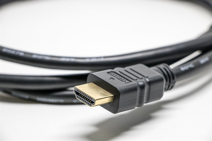
An AI device that has to show something, a camera feed, a result, a user interface, needs to get its display output onto a standard monitor, and the gap is between what the processor drives and what the monitor takes. The processor speaks MIPI DSI, built for a panel a few centimetres away, and the monitor speaks HDMI, built to run down a cable, and the two do not connect directly.
The LT9611UXC converts MIPI DSI to an HDMI output, a bridge that takes the processor's DSI display stream and turns it into an HDMI signal a monitor or a capture device accepts. It handles the formats and the rates a display needs, and it lets a processor that only has a DSI output drive a standard HDMI screen without that capability built into the processor. For a device that has to show its work on an ordinary monitor, the bridge is the part that gets it there.
The bridge has its own demands. The DSI side is a short reach, tightly timed interface that wants the bridge placed close to the processor with short, matched traces, and the HDMI side is a transmission line out to a connector that wants its own careful routing and the right termination. A bridge dropped on the board without attention to either side is a bridge that shows sparkle, blank frames, or nothing.
The resolution and frame rate set how hard the job is. A modest interface at a modest resolution is forgiving, while a high resolution at a high frame rate pushes the data rate up to where every part of the path, the bridge, the traces, and the connector, has to be right. The bridge is chosen for the resolution the device has to drive, with the bandwidth headroom that resolution demands.
The bridge also carries the parts of HDMI beyond the picture. Audio rides the same connector, and the handshakes that let a monitor announce what it can display, the EDID and the link training, are handled by the bridge so the processor does not have to, which is part of what makes a bridge easier to design in than building HDMI into the processor itself.
Switching and routing the high speed lanes
Inside the device, PCIe is how the processor talks to the fast peripherals, an accelerator, an NVMe drive, a fast network controller, and the processor has a fixed number of lanes to spend. When more devices want a lane than there are lanes, or when two devices share a slot that only one uses at a time, the lanes have to be switched or steered rather than hard wired.
The PI2PCIE2412ZHEX switches PCIe lanes, a switch that routes a high speed PCIe lane between destinations so one set of lanes can serve more than one device, or so a design can choose at runtime which device a lane connects to. It passes the high speed signal with the integrity PCIe needs, which is the hard part, since a switch in a high speed path is a place the signal can degrade if the part is not built for the rate.
A lane switch is not a simple multiplexer. At PCIe speeds the switch has to preserve the signal's edges and timing as it passes through, which is why a part made for this is specified for the PCIe generation it supports and adds little of its own degradation. Using an ordinary analog switch in a PCIe path, where the rate is far beyond what it was made for, is how a link trains down to a slower speed or fails to come up at all.
The need for switching is set by the lane budget. A processor with plenty of lanes for every device needs no switch, while one short on lanes uses a switch to share them, at the cost of the switch's own signal budget and the routing it adds. Counting the lanes the processor offers against the devices that want them is what shows whether a switch is needed at all.
Hot plug is the other reason to switch. A design where a device can be inserted or removed while the system runs needs the lane handled so the link comes up and down cleanly, which a switch built for it manages, where a hard wired lane assumes the device is always there. Whether the slot is hot plugged shapes the part as much as the lane count does.
At these speeds the wire is a transmission line
The fact that governs all of this is that a high speed signal does not travel down a trace the way a slow one does, and treating the trace as a plain wire is where high speed designs fail. At the rates HDMI and PCIe run, the signal's wavelength is short enough that the trace behaves as a transmission line, where the width of the trace and its distance from the ground plane set an impedance the signal sees, and any place that impedance changes, a stub, a sharp corner, a connector, a via, reflects part of the signal back and muddies the rest. A trace that is too wide or too narrow, a pair whose two halves are different lengths, a return path broken by a gap in the ground plane, each adds an error that at slow speeds would not matter and at these speeds closes the eye the receiver has to see. The defenses are a discipline, not a fix applied at the end. The differential pairs that carry these signals are routed at a controlled impedance, kept to matched lengths so the two halves arrive together, given a solid unbroken ground beneath them for the return current, and kept away from the noisy parts of the board that would couple into them. The connectors and the vias, the places impedance naturally jumps, are chosen and laid out to disturb the signal as little as they can. None of this shows on a schematic, where the connection is a single line, and all of it decides whether the link works, which is why a high speed design lives or dies in the layout and not in the parts list. A team that picks the right bridge and the right switch and then routes them like slow signals has built a device that fails in a way the schematic cannot explain.
What makes this hard to catch is that it is graded, not pass or fail. A layout that is a little wrong gives a link that works on many units and fails on a few, or works cold and fails warm, which reads as a flaky product rather than a clear fault, and chasing it without the signal integrity view is chasing a ghost. Treating the high speed paths with the discipline up front is far cheaper than finding the margin was thin after the boards are built.
The parts are the easy half. The layout is the design.
Why bridges and switches exist at all
It is fair to ask why a device needs these extra parts instead of the processor just having the right output. The answer is that a processor offers a fixed set of interfaces, chosen by its maker for the common case, and a given device often needs an interface the processor does not have or more of one than it provides. A bridge or a switch fills that gap without forcing a different, more expensive processor.
A bridge converts between two interfaces that carry the same information in different forms, DSI to HDMI being one, and it earns its place when the processor speaks one and the world outside speaks the other. The alternative, a processor with HDMI built in, may cost more or may not exist in the class the device needs, so the bridge is the cheaper path to the same output.
A switch or a retimer addresses distance and fan out rather than format. A switch routes one lane among several destinations, and a retimer, a near relative, cleans up and resends a high speed signal that has degraded over a long run on the board, so a signal can reach a connector at the far edge of a large board still inside spec. Both exist because the processor's lanes are finite and the board is not always small.
Integration is the counter pressure. Each bridge, switch, or retimer is a part, a cost, and a place the signal can degrade, so a design that gets the interface it needs from the processor directly is cleaner than one stitched together from converters. The parts are reached for when the processor cannot do it directly, not in preference to a processor that can.
Protecting the ports from the outside world
A connector that faces the outside world, an HDMI socket a user plugs into, exposes the high speed signal and the chip behind it to whatever arrives on the cable. A static discharge from a finger or a cable can punch through a high speed input built for millivolt swings, and a port with no protection is a failure waiting for the first careless plug.
The defense is protection placed right at the connector. Low capacitance ESD diodes clamp a surge to ground before it reaches the bridge or the switch, and they have to be low capacitance because the signal is high speed, since a protection part that loads the line too heavily degrades the signal it guards. The protection shunts the surge while staying nearly invisible to the data.
Placement is half the protection. The ESD part sits as close to the connector as it can, so the surge is clamped before it travels into the board, and the layout gives it a short, low inductance path to ground, because a clamp on a long thin trace acts too late. Protection added as an afterthought, far from the port, guards far less than it seems to.
The same care covers the power and the hot plug. A port that delivers power, or a connector that is live as a cable goes in, needs protection against a surge or an inrush on those pins too, so the connector is treated as a whole, signals and power together, against everything a user or a cable can do to it.
The cost of a high speed lane on the board
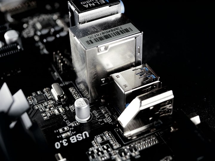
A high speed interface is cheap in parts and dear in the board it demands, and that cost is counted at design time or paid at debug. The controlled impedance these signals need often calls for more board layers, a dedicated ground plane under the signal layer and a stackup designed so the traces see a consistent impedance, and that layer count is a real cost per board.
Length matching is its own work. The two halves of a differential pair are kept the same length within a tight tolerance, and where several pairs run together, like the lanes of a PCIe link, they are matched to each other as well, which fills board area with the small serpentine wiggles that equalize the lengths. A layout tool helps, and the constraint still shapes where everything can go.
Connectors are where the signal leaves the controlled world of the board, and they are chosen for the rate. An HDMI connector and a PCIe slot are specified for their speeds, and a cheap connector or a careless footprint adds a discontinuity right where the signal is least protected, which is why the connector is part of the high speed design and not an afterthought bolted on.
Vias, the holes that move a signal between layers, are small discontinuities that add up. A high speed trace is routed to cross as few layers as it can, and where it must change layers, the via is designed with the neighboring ground vias that give its return current a path, so the jump disturbs the signal as little as possible. A design that routes high speed signals through many casual vias pays for it in a degraded link.
The length of the run sets how much of this matters. A short hop between two close chips forgives a great deal, while a signal that has to cross a large board to a connector at the edge stresses every one of these, and may need a retimer to make it at all. The budget for a high speed lane is drawn over its whole path, from the source pin to the far connector, not at any one point.
Crosstalk is the neighbor problem on a dense board. A high speed pair run too close to another aggressive signal picks up its noise, so the pairs are spaced apart and sometimes guarded, and the routing finds room for that spacing on a board that is already crowded. The space between the high speed pairs is as designed as the pairs themselves.
The clock the link runs on
A high speed serial link carries its own timing in the data, and the chips at each end still run from a reference clock whose quality shows up in the link. A reference clock with too much jitter spreads the timing of every bit and eats into the margin the link has, so a high speed design gives its serializers a clean, low jitter clock from a source chosen for it.
Spread spectrum clocking is the twist that catches teams. To pass emissions limits, many systems deliberately wobble the clock a little to spread its energy across frequencies, and both ends of the link have to be set to track that wobble, since a receiver that expects a steady clock and gets a spread one loses lock. The clocking scheme is decided for the whole link, both ends together, not chip by chip.
The clock source is part of the bill, not free. A high speed link wants an oscillator with a jitter spec to match, and a cheap clock that is fine for slow logic can starve a fast link of margin it cannot get back. The clock is chosen for the fastest link it feeds, and one clean source can serve several links when it has the jitter budget for the fastest among them.
Matching the interface to what the processor offers
The high speed design begins at the processor, because the processor sets which interfaces exist to build on. A processor with a DSI output and a handful of PCIe lanes defines what the device can do directly and what it needs a bridge or a switch to reach, and choosing the processor without checking its high speed interfaces is choosing blind.
The count and the generation both matter. A processor may have PCIe lanes but of an older generation that caps the bandwidth, or a DSI output of a width that limits the resolution it can drive, and a device that needs more than the processor offers has to bridge, switch, or change processors. Reading the processor's high speed interfaces against what the device has to drive and connect is the first step, before any bridge or switch is chosen.
This is why the processor and the high speed parts are chosen together. A bridge that converts from an interface the processor does not have is useless, and a switch for a lane generation the processor does not run is a mismatch, so the parts are picked to fit the processor's real outputs, not an idealized set.
The package and the pins constrain it too. A processor high speed pins come out in a fixed place, and the bridge or switch and its routing have to reach them over a short clean path, so the placement of these parts is decided early, near the processor high speed pins, before the rest of the board fills in around them.
How a high speed link is checked
A high speed link either trains up and runs or it does not, and when it does not, the way to see why is to look at the signal as the receiver sees it. The eye diagram, the signal transitions overlaid on each other, shows an open eye when the link is healthy and a closing one as the margins shrink, and it turns a vague the link is flaky into a measurement of how much margin is left.
The standards that define these interfaces come with compliance tests for this reason. HDMI and PCIe each specify how the signal has to look at defined points, and a design checked against those tests on real hardware is a design known to work rather than hoped to, which matters because a marginal link can pass on one unit and fail on the next from normal part to part variation.
Measuring this needs the right instrument and fixture, an oscilloscope fast enough for the rate and a way to probe the signal without disturbing it, which is its own small cost in a high speed program. Skipping the measurement and trusting that it works because one board did is how a design ships a link that fails in the field on the units that fell the wrong side of the margin.
Margin is what separates a design that ships from one that merely works. A link with healthy margin tolerates the part to part spread, the temperature swing, and the aging a field unit sees, where a link that only just passes on the bench has nothing left for the real world. The aim is not a link that works once, but one with margin to spare.
Questions that come up wiring high speed into a device
Why do I need a bridge to drive an HDMI monitor?
Because many processors output display over MIPI DSI, a short reach panel interface, not HDMI, which a monitor takes. A bridge converts DSI to HDMI so a DSI only processor can drive a standard screen, without paying for a processor that has HDMI built in or doing without the output.
When do I need a PCIe lane switch?
When more devices want a PCIe lane than the processor provides, or when two devices share a connection used one at a time. A switch routes a lane among destinations so the lanes go further. A processor with enough lanes for every device needs no switch.
Why does my high speed link work on the bench but fail in production?
Usually the layout, not the parts. At HDMI and PCIe rates the traces are transmission lines, and small differences in impedance, length matching, ground return, or a connector can close the receiver's eye. A link that is marginal on a good bench board fails when those margins shrink, so the layout has to be right, not lucky.
Can I use a regular analog switch in a PCIe path?
No. PCIe runs far faster than a general purpose analog switch was made for, and such a switch degrades the signal enough that the link trains down or never comes up. Use a switch specified for the PCIe generation, built to pass the rate with little added degradation.
What is a retimer, and when do I need one?
A retimer receives a degraded high speed signal, cleans it up, and resends it fresh, which lets a signal reach across a large board still in spec. You need one when a high speed run is too long for the signal to make the distance cleanly on its own, common on big boards or to far connectors.
How many board layers does a high speed design need?
Enough to give the high speed signals a controlled impedance with a solid ground plane beneath them, which usually means more layers than a simple board. The exact count depends on the number of high speed signals and the stackup, and skimping on layers to save cost is paid back in a link that will not run reliably.
Wiring the high speed paths in order
The order keeps the signal and the routing from being solved separately. Start from the processor and read its high speed interfaces, the display output it drives and the lanes it offers. Match those to what the device has to do, and where there is a gap, choose the bridge that converts the format or the switch that shares the lanes. Place the bridge close to its source with the short side short. Lay out every high speed pair at controlled impedance, matched length, over solid ground, to a connector chosen for the rate. Add a retimer where a run is too long to make on its own.
None of this is reinvented each time. The impedance targets, the length match rules, and the connector choices carry from one high speed design to the next, captured in a set of layout rules the tool enforces, so the discipline is applied consistently rather than rediscovered. A high speed design is repeatable once the rules are written down.
The thread through all of it is that a high speed signal is an analog problem wearing a digital schematic, and the layout carries the design that the parts list only hints at. Get it right and the picture is clean and the lanes train to full speed. Get it wrong and the device sparkles, drops frames, or runs its links slow, for reasons the schematic will never show.