Free Shipping Over$200

- Products
- Marking
- Alternative

Choosing Boot and Data Storage Parts for an Edge Device
An edge device does three different things with memory, and one chip does not do all three well. It has to hold the code it boots and runs, keep the working data the processor churns through while it is on, and store the bulk data that has to survive a power cycle. Each of those is a separate job with a different kind of memory behind it, and choosing storage for an edge device is a matter of matching the memory to the job rather than hunting for one part that does everything.
The parts split along those three jobs. Flash holds code and small persistent data and keeps it through a power loss. Working memory, the RAM, is fast and large enough for the processor to run in but forgets everything when the power drops. Bulk storage holds the data and the files that have to stay. The art is in picking the right type and size for each, and in how the device gets from a cold start to running code, which is the thread that ties the choices together.
Three jobs, three kinds of memory
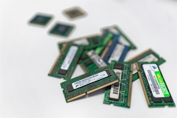
Code storage has to be non volatile and reliable, since a corrupted boot image is a brick, and it can be modest in size because firmware is small next to data. Working memory has to be fast and large enough to hold what the program and the model need at once, and it does not have to remember anything when the power is off. Bulk storage has to be large and survive power cycles, and it can be slower than working memory because it is read and written in blocks rather than run from directly.
Mixing these up is where designs go wrong. Running a program from a part meant for bulk storage is slow and awkward, and trying to hold a model's working set in flash that was sized for code leaves the device thrashing. The first decision is to name the three jobs the device has and size each one, before any part number is chosen.
The split also shapes the board. Three memory jobs can mean three chips, or two, or one part that covers two of them where a processor carries its own RAM or flash on die. Counting the jobs first shows whether the device needs three parts or can fold some together, before the cost and the board area are committed.
The flash that holds the code
Many small edge devices boot from a serial flash on a SPI bus, a part that is cheap, small, and uses few pins. The size is chosen for the firmware plus a margin for updates and a little persistent storage, and the densities run from under a megabyte to tens of megabytes for a part of this kind.
For a middling firmware, the W25Q64JVZEIM gives 64 megabit of SPI NOR flash, a common size that holds a typical edge firmware with room for an over the air update image alongside the running one. It reads quickly enough for a processor to fetch code from it or to copy that code into RAM at boot, and it keeps the pin count low.
Where the code is tiny, a smaller part saves cost and board space. The MX25V1006FZUI is a small density SPI flash for a device whose firmware is measured in kilobytes, a sensor node or a simple controller that needs to store its program and a handful of settings and nothing more. Paying for megabytes a device will never use is a cost with no return.
Where the firmware is large, a bigger part holds it without a second chip. The IS25LP256E-JLLA3 gives 256 megabit of SPI flash, room for a richer firmware, a full update image, and a file system for logs or configuration, on the same simple SPI bus. The density is matched to what the code and its persistent data take, with a margin, and not to a round number.
NOR flash is the right type for code because it can be read byte by byte at random, which is what a processor needs to fetch instructions, and it is reliable in the way a boot image demands. Its weakness is slow writes and a higher cost per bit, which is why it holds code and not bulk data.
The same SPI NOR family spans these densities on one footprint and one driver, which is part of why it is the default for code. A design can move up or down the density range as the firmware grows or shrinks without changing the bus or the software that talks to it, and a second source in the same family is usually a pin for pin swap.
When the code needs to run faster
A plain SPI flash feeds code one bit per clock on a single data line, and for a processor that runs code directly from flash, that can starve it. The fix is a wider, faster path to the same kind of memory.
The IS25WJ064F-JTLE-TR is a QSPI flash that moves data on four lines at once instead of one, several times the read bandwidth of a single line SPI part for a few more pins. It suits a device that executes code in place from flash, or that loads a large image into RAM at boot and wants that boot to be quick, where the extra read speed pays for the extra lines.
For the fastest random reads, a parallel bus still has a place. The S29GL032A90TFIR40 is a parallel NOR flash that puts a full address and data bus on its pins, giving fast random access for a processor that executes in place and cannot tolerate the latency of a serial part. It costs many pins and board area, which is why it shows up where execute in place performance matters more than a small package, often in longer lived industrial designs.
The choice between serial and parallel for code is a choice about pins against latency. A serial part keeps the package small and the routing simple and accepts the latency of clocking code out a few lines at a time, while a parallel part spends pins and area to cut that latency. The processor appetite for instruction bandwidth decides which way the trade falls.
Bulk storage, raw NAND against managed eMMC
When a device has to store more than code, logs, captured data, a model that does not fit in code flash, it needs bulk storage, and that means NAND rather than NOR. NAND packs far more bits per area and costs less per bit, at the price of slower random access and the need to manage its quirks.
The W25N01GVZEIG gives 1 gigabit of SPI NAND flash, much more storage than a NOR part on the same simple SPI bus, for data a device gathers and keeps. Raw NAND like this asks the host to handle bad blocks and wear leveling and error correction in software, which is a real cost in firmware that buys the low part price.
Where the storage is larger or the team would rather not manage raw NAND, a managed part does it for them. The THGAF8G8T23BAIL is eMMC storage for an edge device, NAND with a controller built into the same package that handles the bad blocks, wear leveling and correction itself, presenting a clean block device to the host. It costs more than raw NAND and saves the firmware that would manage it, which is the trade a team makes by how much storage it needs and how much software it wants to own.
Bulk storage is also where a model too large for code flash lives. A device that loads a several megabyte model at boot keeps it in NAND or eMMC and copies it into RAM to run, which makes the bulk store part of the boot path rather than only a data sink, and its read speed part of how fast the device starts.
How much bulk a device needs is set by how long it goes between offloads. A device that ships its data to the cloud each minute needs only a small buffer, while one that records for days offline needs room for all of it plus a margin for a long outage. The capacity follows the worst gap between offloads, not the average.
The working memory the processor runs in
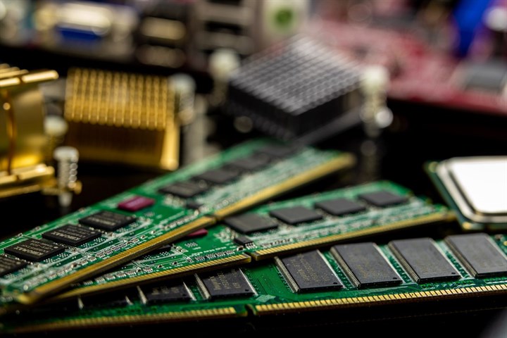
A processor running a real program, and a model, needs working memory that is far faster and larger than flash, and that means RAM. The amount is set by what has to be in memory at once, the program, the model's weights and its working buffers, and the operating system if there is one, and a device short on RAM swaps, stalls, or cannot load its model.
For a modest host, the MT48LC8M16A2P-6A is SDRAM working memory, a straightforward volatile memory that gives a processor room to run, on a parallel bus that many mature microcontrollers and processors drive directly. It fits a design that needs more RAM than the chip has on board but not the bandwidth or capacity of the newer memory types.
For an edge AI processor that moves a lot of data, the K3LK3K30EM-BGCN is LPDDR working memory for edge AI, a low power high bandwidth memory that feeds a hungry processor the data a model needs while drawing less power than older RAM at the same work. It suits a device where the model is large and the memory bandwidth is the thing that limits how fast inference runs, which is common once the model outgrows the on chip memory.
Bandwidth and capacity are separate questions for working memory. A model can fit in a given capacity and still run slowly if the memory cannot feed the processor fast enough, which is the gap between an older parallel memory and LPDDR at the same size. Sizing RAM means asking both how much has to be resident and how fast it has to be read.
The boot path ties it all together
The decision that organizes every memory choice is how the device gets from power on to running code, because the boot path decides what kind of code storage and how much RAM the design needs. At power on the processor runs the first instructions from somewhere non volatile, and there are two broad ways that goes. In execute in place, the processor fetches and runs code directly from NOR flash, which needs a flash fast enough to feed it, a QSPI or a parallel NOR, and which keeps the RAM requirement low because the code is not copied anywhere. In load and run, a small boot stage copies the main code from flash, or from a managed device like eMMC, into RAM and then runs it from there, which is faster once running and needs enough RAM to hold the code plus the working data, but lets the code live in cheaper, denser storage. A device built around a large model and an operating system almost always loads and runs from NAND or eMMC into LPDDR, because the code is too large to execute in place and the RAM is there for the model anyway. A small sensor node often executes in place from a SPI NOR part with little or no separate RAM, because its code is small and adding RAM would be cost with no purpose. The whole memory list, which flash, how much RAM, raw NAND or eMMC, follows from which of these two paths the device takes, so the boot path is decided first and the parts are chosen to serve it.
A hybrid is common in practice. A tiny first stage executes in place from a small NOR flash, just enough code to bring up the RAM and the bulk storage, and then it loads the large main image from eMMC or NAND into RAM and runs that. This is how a device carries a small fast NOR and a large NAND and a big RAM at once, each playing its part in a boot that hands off from one to the next.
Choose the boot path, and the memory map falls out of it.
Surviving a power loss mid write
An edge device loses power at the worst moment, mid write, and what survives that depends on how the storage was designed to handle it. A flash write cut off partway can leave a block half programmed, and a file system that assumed the write finished can come back corrupt, which on the boot device is a brick and on the data device is lost records.
The defenses are known and have to be chosen in. A journaling or copy on write file system keeps the old data intact until the new write completes, so an interrupted write falls back to the last good state rather than a mangled one. A managed device like eMMC handles some of this in its controller, while raw NAND leaves it to the host, which is part of what the host firmware takes on when it picks raw NAND.
The update path is where this bites hardest. An over the air update that is interrupted must not leave the device unable to boot, which is why a safe update keeps the running image until the new one is fully written and verified, and falls back if the power drops mid update. A device that overwrites its only boot image in place is one bad moment from a brick.
Power loss is also why some designs keep a small always intact store. A separate region, or a separate small part, holds the data that must never be lost, written rarely and protected, while the churn of logs and updates happens elsewhere. Splitting the never lose this from the rewrite this often keeps a power cut from taking the data the device could least afford to lose.
Matching density and endurance to the job
Size is chosen against what the job stores plus a margin, and the margin is real work, not a guess. Code flash needs room for the firmware, a second copy for a safe over the air update, and any persistent settings, and a device that fills its flash has no room to update itself safely. Bulk storage is sized for the data the device keeps between offloads, with headroom for the days the network is down and the data piles up.
Endurance is the spec that catches teams who treat all flash as the same. Flash wears out with writes, each cell rated for a number of erase cycles, and a design that writes a log to the same place every second can wear out a cheap part in the field far sooner than anyone planned. NOR and NAND and the managed parts differ in how many writes they take and in whether they spread the wear for you, and a write heavy job needs either a part rated for it or a managed device that levels the wear across its cells.
The read and write pattern matters as much as the total size. A part that is written rarely and read often, like code, asks little of endurance, while a part that logs continuously asks a lot, and the same density part can be right for one and wrong for the other. Naming how each store is written, and how often, is what turns a density number into the right part.
Retention is the quiet companion of endurance. Flash holds its data for years, but that span shrinks as the part wears and as the temperature climbs, and a device that has to keep its data for a decade in a hot enclosure asks more of the flash than a benign desk environment does. The data that has to survive the longest is held in the part with the retention to back it.
These specs trade against cost, and the trade is made per store, not once for the device. The code flash can be a higher grade part because it is small and its integrity is the whole device, while the bulk store can be a cheaper grade because its data is replaceable. Spending evenly across the memory map wastes money where it is not needed and starves it where it is.
Temperature grade rides along with the rest. A device in a hot enclosure or an outdoor cabinet needs memory rated for the temperature it will see, since a commercial grade part that is fine on a bench can lose data or fail early in the heat, and the grade is matched to the environment the device lives in. A part that meets every other spec on a warm bench can still drop data on the day the outdoor cabinet bakes, so the temperature the device will see in service is part of the choice and not an afterthought.
The interface and the pins it costs
Each memory type asks for a different interface, and the interface is part of the choice because it costs pins, board area, and processor support. A SPI flash needs a handful of pins and almost any processor can talk to it, which is why it is the default for code on a small device. A QSPI part needs a few more pins and a processor with a QSPI controller, in return for several times the speed.
Parallel memories, the parallel NOR and the SDRAM, want a full address and data bus, which is many pins and a processor with an external memory controller, and they earn that cost only where their speed or capacity is needed. LPDDR and eMMC need their own dedicated controllers on the processor, so the processor has to be chosen with those interfaces in mind, since a memory the processor cannot talk to is no memory at all.
This is why the memory and the processor are chosen together. The processor's memory controllers set which memories are even possible, and a memory picked without checking the processor supports its interface is a memory that cannot be used, no matter how good its datasheet.
The package matters alongside the pins. A BGA memory like LPDDR or eMMC needs the board layers and the assembly to place and route it, where a small SPI flash in a simple package drops onto almost any board. The memory map is bounded by what the board can build as much as by what the processor can talk to.
Keeping what is in storage secure
Storage holds the things an attacker wants, the firmware to clone or tamper with and the data to steal, and on a connected device that storage is part of the attack surface. A boot image in plain flash can be read out and copied, or replaced with a modified one, unless something stops it.
Secure boot is the defense for the code. The processor checks a signature on the boot image before it runs it, so a tampered or swapped image is rejected, and the root of trust that does the checking sits where it cannot be changed. The flash still holds the code, and the processor refuses to run code that does not carry the right signature.
The data has its own protection. Sensitive data in bulk storage can be encrypted so a part read off a discarded or stolen device gives up nothing, with the keys held in the processor secure element rather than in the flash beside the data. What the storage needs here is set by how much the device invites attack, decided alongside the capacity and the speed.
Secure boot and encryption lean on the processor, not the memory, which is another reason the two are chosen together. A flash cannot sign or check itself, so the security lives in the processor and the memory only holds what the processor protects. A design that needs secure boot picks a processor that offers it before it picks the flash.
Questions that come up choosing edge memory
Why not use one memory chip for everything?
Because code, working data, and bulk storage are different jobs. Code wants reliable non volatile random read, working memory wants speed and is fine being volatile, and bulk storage wants density and low cost per bit. No single type is good at all three, so a device usually carries a flash for code and a RAM for working memory, and a larger flash or eMMC if it stores bulk data.
What is the difference between NOR and NAND flash?
NOR allows fast random reads byte by byte, which suits code a processor executes or fetches, but it costs more per bit and writes slowly. NAND packs far more bits for less money and is faster to write in blocks, which suits bulk data, at the price of slower random access and the need to manage bad blocks and wear. Code goes in NOR, bulk data goes in NAND.
Should I use raw NAND or eMMC?
Raw NAND is cheaper per bit but asks your firmware to handle bad blocks, wear leveling and error correction. eMMC builds that controller into the package and presents a clean block device, costing more but saving the software. Choose by how much storage you need and how much of that management you want to own.
How much RAM does an edge AI device need?
Enough to hold what runs at once, the program, the operating system if any, and the model's weights and working buffers. A device short on RAM cannot load its model or stalls swapping. Size it from the model and software footprint, and pick SDRAM for a modest host or LPDDR where bandwidth limits inference speed.
What is execute in place, and when do I want it?
Execute in place runs code directly from NOR flash without copying it to RAM, which keeps the RAM requirement low and suits small devices with small code. It needs a flash fast enough to feed the processor, a QSPI or parallel NOR. Larger devices instead load code into RAM and run it from there, which is faster once running and needs more RAM.
Why does my flash wear out in the field?
Flash cells take a limited number of erase cycles, and a job that writes the same area often, like a per second log, can exhaust a cheap part far sooner than expected. Use a part rated for the write load, or a managed device that spreads the wear across its cells, and size the store so writes are not concentrated.
Choosing the memory in order
The order keeps the parts from being chosen against each other. Name the three jobs the device has, code, working memory, and bulk storage, and size each. Decide the boot path, execute in place or load and run, since it sets the kind of code flash and the amount of RAM. Pick the code flash for the firmware size and the read speed the boot path needs. Pick the RAM for what runs at once. Add bulk storage, raw NAND or eMMC, if the device keeps data. And check the processor's interfaces support every memory chosen, because that is what makes them usable.
None of this adds parts a device did not need. A small node still ends with one flash and maybe no separate RAM, and a rich device ends with the flash, the RAM, and the bulk store it always required. The order only makes sure each is the right type and size, and that the processor can talk to all of them.
The thread through all of it is that an edge device's memory is a small system, not a single part, and the boot path is the spine that the rest hangs from. Get the map right and the device boots, runs its model, and keeps its data for as long as it has to. Get it wrong and the device is slow, out of memory, or worn out before its time.