- Products
- Marking
- Alternative
Texas Instruments 1P1G08MDBVREPG4

- Part No.:
- 1P1G08MDBVREPG4
- Manufacturer:
- Texas Instruments
- Category:
- Gates and Inverters
- Package:
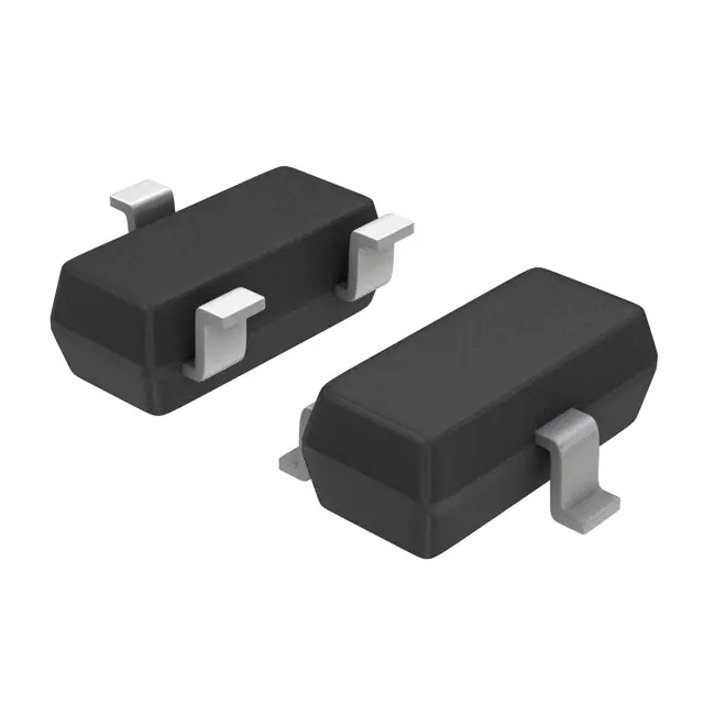
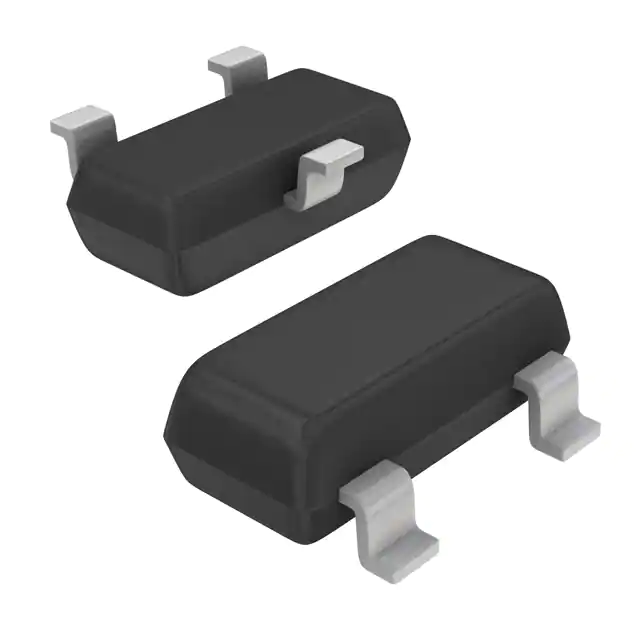
- SC-74A, SOT-753
- Datasheet:
-
 1P1G08MDBVREPG4.pdf
- Description:
- IC GATE AND 1CH 2-INP SOT23-5
- Quantity:
Unit Price:$0.000000
Ext Price:$0.000000
- Payment:

- Shipping:

Inventory:0
Send us your inquiry,we will respond immediately.
In Stock : 0 PCS
| Qty. | Unit Price | Ext Price |
| 0+ | $0.000000 | $0.000000 |
*Products eligible for online ordering ship within 1-2 business days,please contact us for exact shipping times.
Also you can RFQ for 1P1G08MDBVREPG4 or email to us: Email: [email protected] , we will contact you within 12 hours.
Product Details
1P1G08MDBVREPG4 (Texas Instruments SN74LVC1G08-EP) - Single 2-Input AND Gate with Ioff Partial-Power-Down, Pb-Free SOT-23-5
1P1G08MDBVREPG4 is the InFortune ordering code for the Pb-free / RoHS "G4" option of the Texas Instruments SN74LVC1G08-EP single 2-input AND gate. Beyond the AND function (Y = A AND B), this page highlights what makes the LVC gate a clean mixed-voltage interface part: 5.5 V-tolerant inputs, Ioff partial-power-down protection, a strong ±24 mA output at 3.3 V, and operation from 1.65 V to 5.5 V in a 5-pin SOT-23 (DBV). It suits battery, IoT, medical and communications boards that mix supply rails and power sections up and down independently.
Product Introduction
The SN74LVC1G08-EP is a single 2-input positive-AND gate - output high only when both inputs are high - and the "G4" suffix on this order code simply denotes the Pb-free, RoHS-compliant second-level-interconnect finish. It is the same silicon and the same data-sheet specification as the standard order option; the G4 designation is a packaging/lead-finish trait, chosen by buyers who standardise on green ordering codes.
Where this gate earns its place on modern boards is as a mixed-voltage interface. Its inputs accept up to 5.5 V regardless of VCC, so a 1.8 V or 3.3 V-powered gate can read signals from a 5 V domain directly; and its Ioff circuit disables the output when the device is unpowered, so it will not load or back-drive a bus that is still alive. Combined with the wide 1.65 V–5.5 V supply, that makes it a safe glue-logic element between blocks running on different rails.
It also drives hard for its size - ±24 mA at 3.3 V - switches with a 3.6 ns typical-max delay at 3.3 V, and idles at about 10 µA, so it fits power-sensitive portable and IoT designs as easily as line-powered ones.
Expert Technical Insight
Using the LVC single AND gate as a mixed-voltage / partial-power-down element:
- 5.5 V-tolerant inputs simplify level interfacing: because the inputs tolerate voltages above VCC, a 3.3 V-powered gate can AND two 5 V control lines without a separate level shifter - just keep the output rail at the destination logic level.
- Ioff protects partially-powered systems: in a design where one rail sleeps while another stays on, Ioff ensures the unpowered gate's output goes high-impedance instead of clamping or leaking, which prevents back-current and protects both the gate and the live bus.
- "G4" vs the base code is a finish, not a different part: 1P1G08MDBVREPG4 and 1P1G08MDBVREP are the same SN74LVC1G08-EP die and specification; G4 only marks the Pb-free/green ordering. Choose by your procurement standard, not by expecting different electrical behaviour.
Key Benefits
Inputs accept voltages above VCC, so a 1.8 V or 3.3 V gate reads 5 V signals directly - mixed-voltage interfacing without a level shifter.
Outputs go high-impedance when unpowered, preventing back-current into a still-live bus in multi-rail and sleep-mode designs.
Strong 3.3 V drive with about 10 µA quiescent current suits both portable and line-powered boards.
Green ordering option of the SN74LVC1G08-EP, identical die and specification, for buyers standardising on Pb-free codes.
Specifications
| Parameter | Value | Conditions / Notes |
|---|---|---|
| Device Type | Single 2-input positive-AND gate (Enhanced Product) | One channel; LVC family; Pb-free (G4) |
| Manufacturer | Texas Instruments | SN74LVC1G08-EP (data sheet SCES454C) |
| Logic Function | Y = A AND B | Output high only when A and B are both high |
| Supply Voltage (VCC) | 1.65 V to 5.5 V | Data retention down to 1.5 V |
| Input Tolerance | Up to 5.5 V | Inputs accept voltages above VCC (mixed-voltage) |
| Ioff (partial power down) | ±10 µA max | VI/VO = 5.5 V, VCC = 0 |
| Output Drive (IOH/IOL) | ±24 mA at 3.3 V | ±32 mA at 4.5 V |
| Quiescent Current (ICC) | 10 µA max | Full VCC range |
| Propagation Delay (tpd) | 3.6 ns max at 3.3 V | I-temp, CL = 15 pF |
| Input Leakage (II) | ±5 µA max | VI = 5.5 V or GND |
| Input Capacitance (Ci) | 4 pF typ | VCC = 3.3 V |
| ESD (HBM / MM / CDM) | 2000 V / 200 V / 1000 V | Exceeds JESD22 |
| Operating Temperature (TA) | −55 °C to +125 °C | M-temp (EP) |
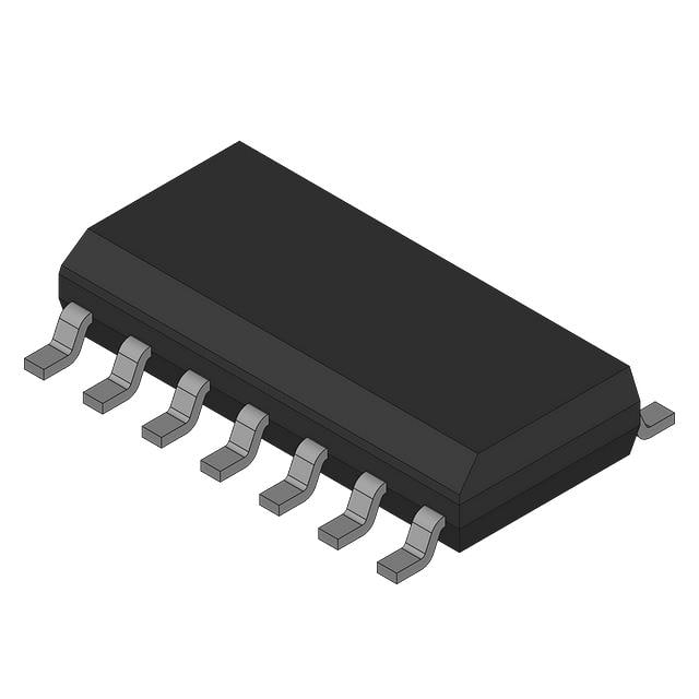
| Package | 5-pin SOT-23 (DBV), Pb-free | Order code SN74LVC1G08MDBVREPG4 |
Note: Values are from the Texas Instruments SN74LVC1G08-EP data sheet (SCES454C); the G4 code shares this specification and differs only in lead finish. Confirm parameters against the latest data sheet before committing a design.
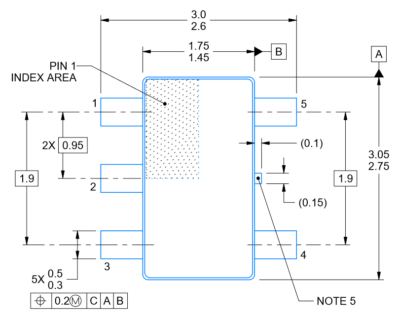
Package Information
This order option uses the DBV 5-pin SOT-23 (JEDEC MO-178, 1.45 mm max height) with a Pb-free, RoHS-compliant finish - the meaning of the "G4" suffix. Mechanically and electrically it is identical to the standard SN74LVC1G08MDBVREP; only the second-level-interconnect finish is specified as green. It is shipped tape-and-reel for automated assembly.
The dimensioned drawing below gives the SOT-23-5 body and lead geometry for the land pattern and reflow profile.
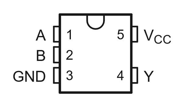
Pin Configuration (SOT-23-5)
Five pins carry the two inputs, the output and the supply pair (top view):
- Pin 1 – A (Input): First AND input; tolerant to 5.5 V for mixed-voltage use.
- Pin 2 – B (Input): Second AND input; tolerant to 5.5 V.
- Pin 3 – GND: Ground (0 V) reference.
- Pin 4 – Y (Output): AND output; disabled by Ioff when VCC = 0; ±24 mA at 3.3 V.
- Pin 5 – VCC: Supply, 1.65 V to 5.5 V; set this rail to the desired output logic level and decouple locally.
Alternative Parts
The first row is the same device under its base (non-G4) order code; the rest are single 2-input AND gates in other logic families. Match the supply range, input tolerance and speed to your interface - only LVC and similar 5 V-tolerant families suit direct mixed-voltage use.
| Part Number | Brand | Family / Type | Package | Note |
|---|---|---|---|---|
| 1P1G08MDBVREP | Texas Instruments | LVC AND (EP) | SOT-23-5 | Same device, base order code (non-G4 finish) |
| SN74AHCT1G08DCKT | Texas Instruments | AHCT AND | SC-70 | TTL-level inputs at 5 V |
| SN74AUP1G08DRYR | Texas Instruments | AUP AND | SON | Ultra-low-power for battery / IoT |
| SN74AUC1G08DCKRG4 | Texas Instruments | AUC AND | SC-70 | Sub-2 V, highest speed |
Logic Family Comparison
| Family | Supply Range | Input Tolerance | Use When |
|---|---|---|---|
| LVC (this part) | 1.65–5.5 V | 5.5 V-tolerant | Mixed-voltage, high drive, Ioff |
| AHCT | 4.5–5.5 V | TTL-level | 5 V TTL interfacing |
| AUP | 0.8–3.6 V | Limited | Battery / IoT, lowest power |
| AUC | 0.8–2.7 V | Limited | Sub-2 V core logic |
Manufacturer Information
Texas Instruments (TI, NASDAQ: TXN), of Dallas, Texas, is a leading logic maker; its LVC family is the workhorse choice for wide-supply, 5 V-tolerant, mixed-voltage interfacing, and the Enhanced-Product (EP) variant adds an extended-temperature, controlled-baseline pedigree. Order codes ending in "G4" denote the Pb-free / green finish of the same device.
The governing document is the SN74LVC1G08-EP data sheet (SCES454C), which defines the electrical limits, Ioff behaviour and the DBV package; lead-finish details are in the package addendum. InFortune Electronics supplies the device under code 1P1G08MDBVREPG4 and provides sourcing and technical support.
Application Areas


Frequently Asked Questions (FAQ)
What is the difference between 1P1G08MDBVREPG4 and 1P1G08MDBVREP?
They are the same SN74LVC1G08-EP die with the same data-sheet specification. The "G4" suffix only denotes the Pb-free / RoHS green second-level-interconnect finish; choose by your procurement standard.
Can the inputs be driven above VCC (5 V into a 3.3 V gate)?
Yes. The inputs are tolerant up to 5.5 V regardless of VCC, so a 3.3 V- or 1.8 V-powered gate can read 5 V logic directly, enabling mixed-voltage interfacing without a level shifter.
What does Ioff / partial-power-down do here?
When the gate's VCC is at 0 V, the Ioff circuit disables the output (high-impedance), so it does not back-drive or load a bus that remains powered - key for systems that power sections up and down separately.
What are its supply range, drive and speed?
It runs from 1.65 V to 5.5 V, drives ±24 mA at 3.3 V, switches in 3.6 ns (max, 3.3 V), and draws about 10 µA maximum quiescent current.
Disclaimer
Information Accuracy: Technical specifications on this page are based on the Texas Instruments SN74LVC1G08-EP data sheet (SCES454C). We strive for accuracy and completeness, but specifications are subject to change without notice.
Product Authenticity: We guarantee all products are genuine factory originals with complete material traceability.
Technical Support: Free technical consultation is available before and after purchase.
Application Note: This product page is for reference only. Suitability for a specific application should be verified by design engineers against actual system requirements.
1P1G08MDBVREPG4 Specifications
- Specifications
- Attributes
- Property Value
- Manufacturer
- Texas Instruments
- Series:
- -
- Package/Case:
- SC-74A, SOT-753
- Packaging:
- Tape & Reel (TR)
- Part Status:
- Discontinued
- Logic Type:
- AND Gate
- Number of Circuits:
- 1
- Features:
- -
- Voltage - Supply:
- 1.65V ~ 5.5V
- Current - Quiescent (Max):
- 10 µA
- Current - Output High, Low:
- 32mA, 32mA
- Input Logic Level - Low:
- 0.7V ~ 0.8V
- Number of Inputs:
- 2
- Input Logic Level - High:
- 1.7V ~ 2V
- Max Propagation Delay @ V, Max CL:
- 5ns @ 5V, 50pF
- Supplier Device Package:
- SOT-23-5
- Operating Temperature:
- -55°C ~ 125°C
- Mounting Style:
- Surface Mount
- Grade:
- -
- Qualification:
- -
- Category:
- Gates and Inverters
1P1G08MDBVREPG4 Relevant information
- 1P1G08MDBVREPG4 Tags
- Popular Search
The following parts are popular search parts in Gates and Inverters.
The Posts
-
Exploring the Features of AN431AN - ATRG1 Voltage Reference IC
The AN431AN - ATRG1 is a significant voltage reference integrated circuit (IC) that plays a crucial role in maintaining stable voltage levels within electronic circuits. Engineered with precision, it o…
-
Unveiling the Wonders of XP1002000 - 05R Electronic Component
The XP1002000 - 05R is an electronic component that stands out for its specialized design and functionality, catering to a variety of electronic system requirements.Unique FeaturesOne of the most notab…
-
Unraveling the Wonders of MMBF170LT1 Transistor
The MMBF170LT1 is a remarkable transistor that has carved a niche for itself in the electronic component landscape. This tiny yet powerful device is engineered with precision to deliver outstanding per…
-
Unveiling the Marvels of MMBF170LT3G Transistor
The MMBF170LT3G is a high - performance transistor that stands out in the realm of electronic components. Engineered with precision, it brings a set of features that make it a valuable asset in numerou…
-
Unveiling the Features of RD16E - T1 - AZ Electronic Component
The RD16E - T1 - AZ is an electronic component that brings a set of unique features to the table. Its design showcases precision engineering, catering to specific requirements in various electronic set…
-
Unveiling the Capabilities of RD16ES - T1 - AZ Electronic Component
The RD16ES - T1 - AZ is a remarkable electronic component that combines advanced technology with practical design to meet the demands of diverse electronic projects.Electrical FeaturesOne of the key as…
Related Products
-
74VHC86MX
Fairchild Semiconductor
-
74VHCT08AM
Fairchild Semiconductor

-
MM74HC02SJ
Fairchild Semiconductor
-
SN74ALS32DB
Texas Instruments
-
SN74ALS86NE4
Texas Instruments
-
74VHCT04AM
Fairchild Semiconductor

-
74HC21DB,112
NXP Semiconductors

-
NLVLCX08DTR2G
Cypress Semiconductor Corp
-
74LVX02M
Fairchild Semiconductor
-
74VHCT00AM
Fairchild Semiconductor
-
XC7WH14DP,125
NXP USA Inc.
-
74HCT4075D,652
Nexperia USA Inc.