- Products
- Marking
- Alternative
Analog Devices Inc./Maxim Integrated MAX5183BEEI+

- Part No.:
- MAX5183BEEI+
- Manufacturer:
- Analog Devices Inc./Maxim Integrated
- Category:
- Digital to Analog Converters (DAC)
- Package:
- 28-SSOP (0.154", 3.90mm Width)
- Datasheet:
-
 MAX5183BEEI+.pdf
- Description:
- IC DAC 10BIT V-OUT 28QSOP
- Quantity:
Unit Price:$0.000000
Ext Price:$0.000000
- Payment:

- Shipping:

Inventory:946
Send us your inquiry,we will respond immediately.
In Stock : 946 PCS
| Qty. | Unit Price | Ext Price |
| 0+ | $0.000000 | $0.000000 |
*Products eligible for online ordering ship within 1-2 business days,please contact us for exact shipping times.
Also you can RFQ for MAX5183BEEI+ or email to us: Email: [email protected] , we will contact you within 12 hours.
Product Details
MAX5183BEEI+ - Maxim MAX5183 Dual 10-Bit 40 MHz Voltage-Output DAC, Simultaneous Differential Outputs, Internal 1.2 V Reference, +2.7 V to +3.3 V, 28-Pin QSOP | MAX5183
MAX5183BEEI+ is the lead-free 28-pin QSOP version of Maxim's MAX5183, a dual, 10-bit, 40 MHz, simultaneous-output digital-to-analog converter that delivers a differential voltage output on each channel through on-chip precision resistors. Built for I/Q signal reconstruction, it pairs two matched DACs with a 10-bit parallel data bus (D0-D9), an internal 1.2 V low-noise bandgap reference, and a 70 dB spurious-free dynamic range at fOUT = 2.2 MHz, while idling in standby or full-shutdown to save power. Running from a single +2.7 V to +3.3 V rail over -40 °C to +85 °C, it suits communications transmitters, DSP, arbitrary-waveform generation and imaging.
Product Introduction
The MAX5180/MAX5183 from Maxim Integrated (now part of Analog Devices) are dual, 10-bit, simultaneous-update digital-to-analog converters designed for the analog signal reconstruction that communications systems demand - low distortion, low power, two channels that move together. The MAX5183 is the voltage-output member of the pair: it carries on-chip precision resistors that turn the core current output into a differential voltage on OUT_P/OUT_N, where the MAX5180 leaves the output as current. MAX5183BEEI+ is the RoHS ("+") option in the 28-pin QSOP.
The signal path is built for I and Q. Both DACs share a single 10-bit parallel bus (D0-D9) clocked by CLK, and they update simultaneously - the reason gain and phase between the two channels are held to ±0.5 %FSR and ±0.2°, the matching a quadrature modulator lives or dies on. Reconstruction quality is set by a 70 dB spurious-free dynamic range (fOUT = 2.2 MHz), -60 dB DAC-to-DAC isolation and the internal 1.2 V low-noise bandgap reference, which can be overridden through REFR/REFO when a system reference is preferred.
Power is managed in three states rather than one. DACEN and PD together select normal operation, a fast-wake standby, or a deep full shutdown - so an I/Q transmitter can drop the converters between bursts and bring them back quickly. The part runs from a single 2.7 V to 3.3 V supply (separate AVDD/DVDD and AGND/DGND for clean analog-digital separation), and the whole device fits the compact 28-pin QSOP over the -40 °C to +85 °C extended range.
Expert Technical Insight
What makes the dual DAC work for I/Q, and where does the board design matter?
- Simultaneous update is the whole point: both DACs latch on the same clock edge, so I and Q never skew. Drive D0-D9 and CLK with clean, equal-length traces; any timing skew you add externally is skew the ±0.2° phase match cannot remove. Treat the bus as a matched group, not ten independent nets.
- The voltage output rides on precision resistors - load them lightly: the on-chip 400 Ω network sets the differential voltage, so present OUT_P/OUT_N to a high-impedance, well-matched differential load (a balun or a diff-amp), keep the two sides symmetric, and the -60 dB channel isolation survives to the board edge.
- Split the supplies and the grounds the way the pinout asks: AVDD/AGND and DVDD/DGND are separate for a reason - bypass each at its pin, join the grounds at one point under the part, and bypass CREF1/CREF2 and REFO so the 1.2 V reference noise does not modulate the SFDR.
Key Benefits
Two 10-bit DACs that latch on the same clock edge hold ±0.5 %FSR gain and ±0.2° phase match - the matching an I/Q modulator needs.
On-chip precision resistors give a ready differential voltage on OUT_P/OUT_N - no external I-to-V network, where the MAX5180 leaves current output.
A 70 dB spurious-free dynamic range (fOUT = 2.2 MHz) and -60 dB DAC-to-DAC isolation keep reconstructed signals clean at the full 40 MHz update rate.
An internal 1.2 V low-noise bandgap reference plus standby and full-shutdown modes, all from a single 2.7-3.3 V supply in 28-pin QSOP.
Specifications
| Parameter | Value | Condition / Note |
|---|---|---|
| Device Type | Dual 10-Bit DAC | Simultaneous-output, voltage |
| Manufacturer | Maxim Integrated (Analog Devices) | MAX5183 |
| Resolution | 10 bits | Per channel |
| Channels | 2 (dual) | Simultaneous update |
| Update Rate | 40 MHz | Max clock |
| Output Type | Differential voltage | On-chip resistors; MAX5180 = current |
| Interface | 10-bit parallel (D0-D9) | Clocked by CLK |
| Reference | Internal 1.2 V bandgap | Low-noise; REFR/REFO external option |
| SFDR | 70 dB | fOUT = 2.2 MHz |
| DAC-to-DAC Isolation | -60 dB | fOUT = 2.2 MHz |
| Gain / Phase Match | ±0.5 %FSR / ±0.2° | Between DAC outputs |
| DNL | ±0.5 LSB | Guaranteed monotonic |
| Settling Time | 25 ns | To ±0.5 LSB |
| Supply Voltage | +2.7 V to +3.3 V | AVDD / DVDD |
| Power Modes | Normal / Standby / Shutdown | Via DACEN, PD |
| Operating Temperature | -40 to +85 °C | Extended (EI grade) |
| Package | 28-Pin QSOP | Outline 21-0055 |
| Orderable Part Number | MAX5183BEEI+ | Pb-free |
Note: Values are taken from the Maxim MAX5180/MAX5183 datasheet. Confirm every parameter against the latest official documentation before committing a design.
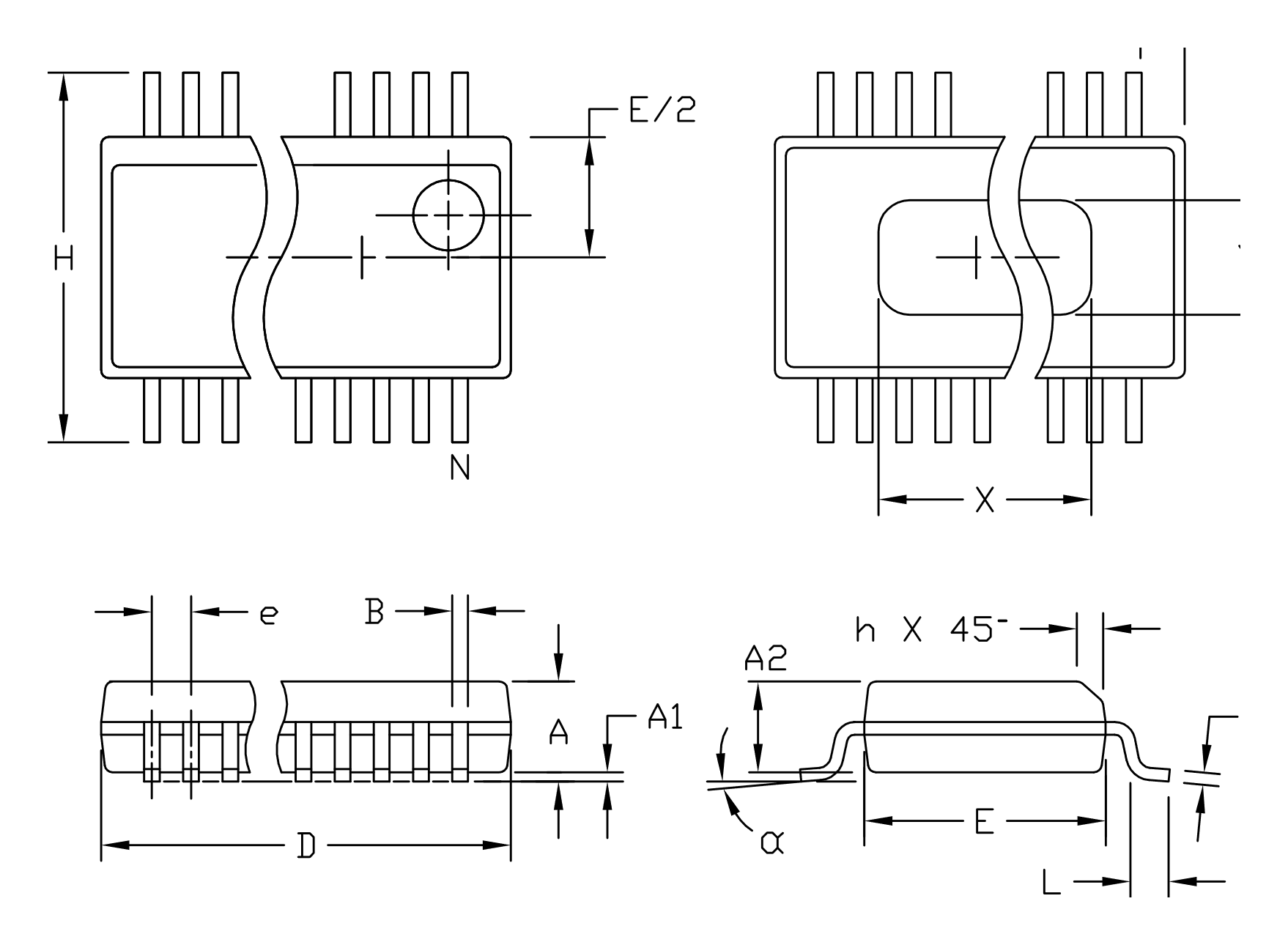
Package Information
MAX5183BEEI+ ships in the 28-pin QSOP (Quarter-Size Outline Package, outline 21-0055) - a 0.150-inch-wide body on 0.025-inch pin pitch that holds 28 leads in roughly the footprint of a 16-lead SOIC, which is why a dual converter with a full 10-bit bus fits where board space is tight. Because the two channels share one package, the analog and digital domains must stay apart on the board: bypass AVDD and DVDD at their own pins, keep the OUT1/OUT2 differential pairs symmetric and away from the D0-D9 bus and CLK, and bypass the CREF1/CREF2 and REFO reference pins close in. The dimensional drawing below gives the full mechanical detail.
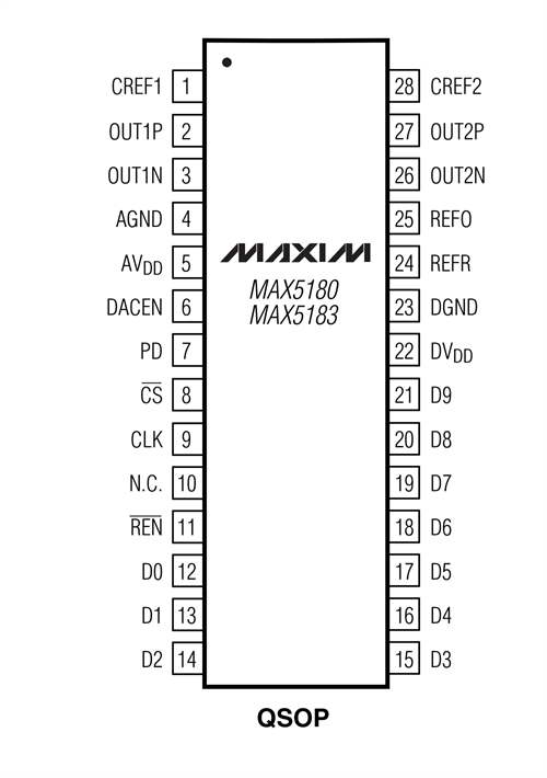
Pin and Signal Definition
The 28-pin QSOP groups the two analog channels on the outer ends and the digital bus along one side (per the MAX5180/MAX5183 datasheet):
- Pins 2, 3 - OUT1P, OUT1N: DAC1 differential analog output (voltage output on MAX5183).
- Pins 27, 26 - OUT2P, OUT2N: DAC2 differential analog output (voltage output on MAX5183).
- Pins 1, 28 - CREF1, CREF2: Reference bias bypass for DAC1 and DAC2.
- Pin 24 - REFR: Reference input. Pin 25 - REFO: Reference output (internal 1.2 V bandgap).
- Pin 11 - REN̅: Active-low reference enable; tie to DGND to activate the on-chip 1.2 V reference.
- Pins 12-21 - D0...D9: 10-bit parallel data input, D0 = LSB, D9 = MSB.
- Pin 9 - CLK: Clock input. Pin 8 - CS̅: Active-low chip select.
- Pin 6 - DACEN, Pin 7 - PD: DAC-enable and power-down select - together choose normal, standby or shutdown.
- Pins 5, 22 - AVDD, DVDD: Analog and digital +2.7 V to +3.3 V supplies. Pins 4, 23 - AGND, DGND: Analog and digital grounds.
- Pin 10 - N.C.: No connect - do not connect to this pin.
Alternative and Related Parts
The closest options are the current-output twin and the rest of Maxim's dual/communications DAC line. Match output type, resolution and interface to your signal chain before substituting.
| Part Number | Brand | Type / Key Difference | Package | Note |
|---|---|---|---|---|
| MAX5180BEEI | Maxim | Same DAC, current output | 28-QSOP | Current-output twin of MAX5183 |
| MAX5181BEEG | Maxim | Dual 10-bit communications DAC | QSOP | Family variant |
| MAX5182BEEI+ | Maxim | Dual 10-bit voltage-output DAC | 28-QSOP | Related dual DAC |
| MAX5170AEEE | Maxim | Single 14-bit serial DAC | 16-QSOP | Higher resolution, serial |
| MAX5176AEEE+ | Maxim | Single 12-bit DAC, voltage output | 16-QSOP | Single-channel option |
Selection Tips: Stay with the MAX5183 for a ready differential voltage output; choose the MAX5180 when your modulator wants the raw current output. Step to the MAX5170/MAX5176 when one channel and higher resolution matter more than the dual, 40 MHz I/Q pairing. Confirm the parallel-bus timing budget against your DSP before locking the layout.
Manufacturer Information
Maxim Integrated, now part of Analog Devices, Inc. (ADI), built the MAX5180/MAX5183 for the demanding corner of data conversion where two channels must track each other through a 40 MHz reconstruction - the I/Q transmit path of a communications system, where channel match, not just per-channel linearity, sets the achievable image rejection.
ADI maintains the datasheet, dynamic-performance plots (SFDR, THD, channel isolation) and the layout and reference-bypass guidance for the family - the documentation that turns the ±0.2° phase match on the data sheet into image rejection on the bench.
Applications
Frequently Asked Questions
How does MAX5183 differ from the MAX5180?
They are the same dual, 10-bit, 40 MHz simultaneous-output DAC. The MAX5183 includes on-chip precision resistors to give a ready differential voltage output on OUT_P/OUT_N; the MAX5180 leaves the raw current output for an external I-to-V network. Choose by what your modulator or amplifier wants to see.
Why does the dual, simultaneous update matter for I/Q?
Both DACs latch on the same clock edge, so the I and Q channels never skew in time. That is what holds the ±0.2° phase and ±0.5 %FSR gain match between channels - the matching a quadrature modulator needs to reject the sideband image. Two separate DACs would not track as tightly.
Does it have an internal reference?
Yes - an internal 1.2 V low-noise bandgap reference, enabled by tying REN̅ to DGND. You can also drive a system reference through REFR / REFO. Bypass CREF1, CREF2 and REFO close to their pins so reference noise does not degrade the 70 dB SFDR.
What interface and supply does it use?
A 10-bit parallel data bus (D0-D9) clocked by CLK, with CS̅ chip-select, running from a single +2.7 V to +3.3 V supply (separate AVDD/DVDD). DACEN and PD select normal, standby or full-shutdown power states. The package is the 28-pin QSOP, rated -40 °C to +85 °C.
Disclaimer
Information Accuracy: The specifications on this page are based on the official Maxim MAX5180/MAX5183 datasheet. We work to keep the information accurate and complete, but parameters can change with product revisions, so design engineers should verify all values against the latest official documentation before final design.
Product Authenticity Guarantee: All parts we supply are genuine factory originals with full material traceability.
Technical Support: Pre-sales and post-sales technical consultation is available free of charge.
Application Notice: This page is for reference only. Suitability for a specific application should be confirmed by the design engineer against the actual system requirements.
MAX5183BEEI+ Specifications
- Specifications
- Attributes
- Property Value
- Manufacturer
- Analog Devices Inc./Maxim Integrated
- Series:
- -
- Package/Case:
- 28-SSOP (0.154", 3.90mm Width)
- Packaging:
- Tube
- Part Status:
- Active
- Programmable:
- Not Verified
- Number of Bits:
- 10
- Settling Time:
- 25µs (Typ)
- Output Type:
- Voltage - Unbuffered
- Differential Output:
- Yes
- Grade:
- -
- Data Interface:
- Parallel
- Reference Type:
- External, Internal
- Number of D/A Converters:
- 2
- Voltage - Supply, Analog:
- 2.7V ~ 3.3V
- Voltage - Supply, Digital:
- 2.7V ~ 3.3V
- Mounting Style:
- Surface Mount
- INL/DNL (LSB):
- ±0.5, ±0.5
- Qualification:
- -
- Supplier Device Package:
- 28-QSOP
- Architecture:
- Current Source
- Operating Temperature:
- -40°C ~ 85°C
- Category:
- Digital to Analog Converters (DAC)
MAX5183BEEI+ Relevant information
- MAX5183BEEI+ Tags
- Popular Search
The following parts are popular search parts in Digital to Analog Converters (DAC).
The Posts
-
Exploring the Features of AN431AN - ATRG1 Voltage Reference IC
The AN431AN - ATRG1 is a significant voltage reference integrated circuit (IC) that plays a crucial role in maintaining stable voltage levels within electronic circuits. Engineered with precision, it o…
-
Unveiling the Wonders of XP1002000 - 05R Electronic Component
The XP1002000 - 05R is an electronic component that stands out for its specialized design and functionality, catering to a variety of electronic system requirements.Unique FeaturesOne of the most notab…
-
Unraveling the Wonders of MMBF170LT1 Transistor
The MMBF170LT1 is a remarkable transistor that has carved a niche for itself in the electronic component landscape. This tiny yet powerful device is engineered with precision to deliver outstanding per…
-
Unveiling the Marvels of MMBF170LT3G Transistor
The MMBF170LT3G is a high - performance transistor that stands out in the realm of electronic components. Engineered with precision, it brings a set of features that make it a valuable asset in numerou…
-
Unveiling the Features of RD16E - T1 - AZ Electronic Component
The RD16E - T1 - AZ is an electronic component that brings a set of unique features to the table. Its design showcases precision engineering, catering to specific requirements in various electronic set…
-
Unveiling the Capabilities of RD16ES - T1 - AZ Electronic Component
The RD16ES - T1 - AZ is a remarkable electronic component that combines advanced technology with practical design to meet the demands of diverse electronic projects.Electrical FeaturesOne of the key as…
Related Products
-
MCP47A1T-A0E/LT
Microchip Technology

-
MCP4706A0T-E/CH
Microchip Technology
-
MCP4716A0T-E/MAY
Microchip Technology
-
MCP4716A0T-E/CH
Microchip Technology
-
MCP4726A0T-E/CH
Microchip Technology
-
MCP4725A0T-E/CH
Microchip Technology
-
MCP4725A1T-E/CH
Microchip Technology
-
MCP4725A2T-E/CH
Microchip Technology
-
MCP4726A1T-E/CH
Microchip Technology
-
MCP4726A3T-E/CH
Microchip Technology
-
MCP4726A2T-E/CH
Microchip Technology
-
MCP4726A0T-E/MAY
Microchip Technology