- Products
- Marking
- Alternative
Analog Devices Inc. LTC3568EDD#PBF

- Part No.:
- LTC3568EDD#PBF
- Manufacturer:
- Analog Devices Inc.
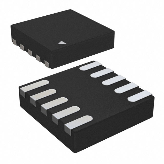
- Package:
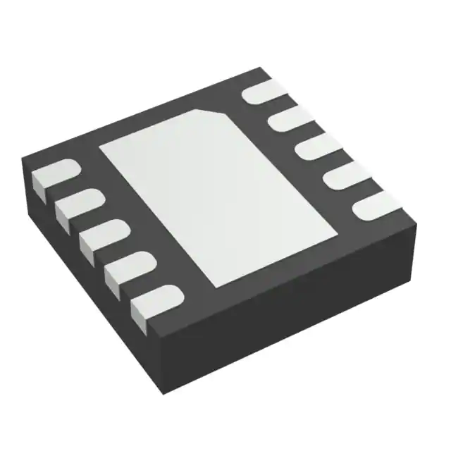
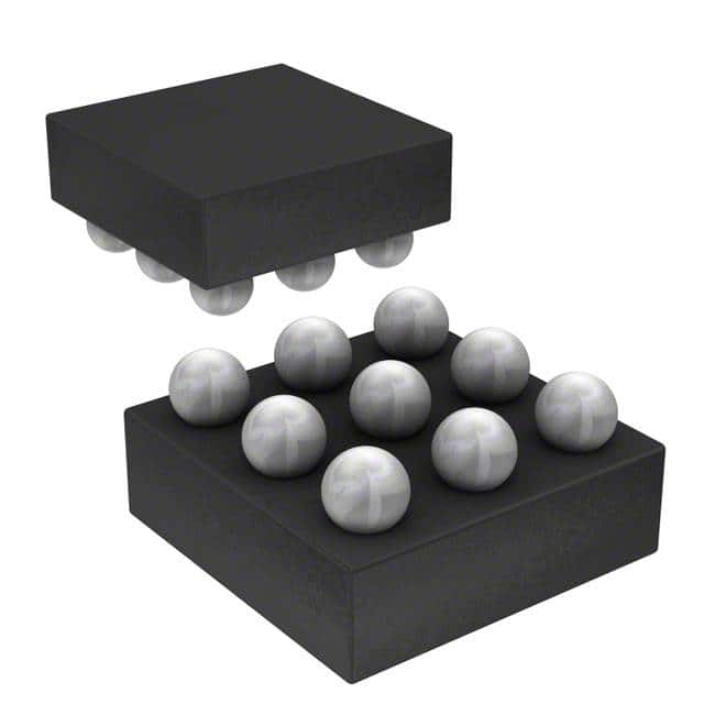
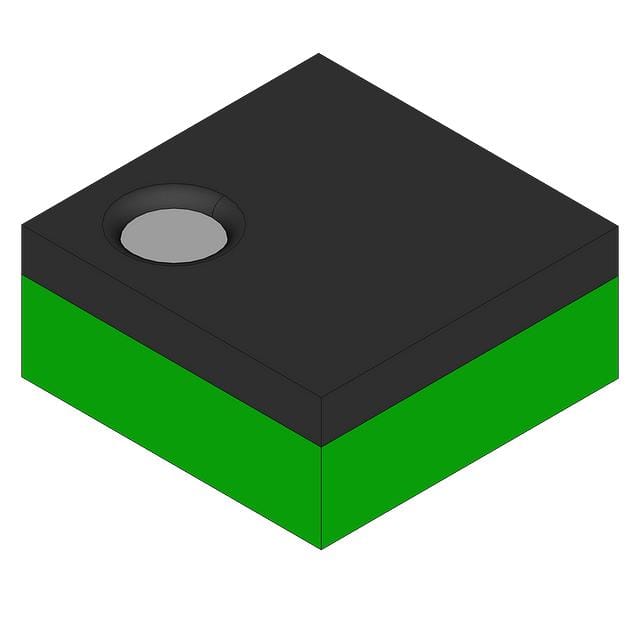
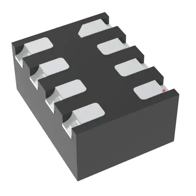
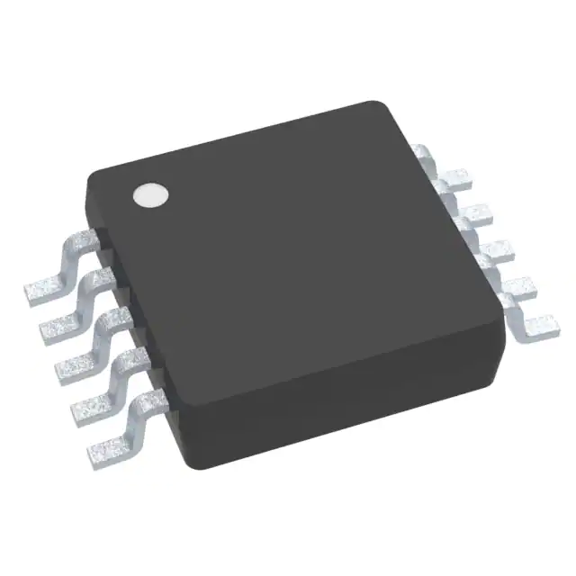
- 10-WFDFN Exposed Pad
- Datasheet:
-
 LTC3568EDD#PBF.pdf
- Description:
- {"@context": "https://schema.org","@type": "BreadcrumbList","itemListElement": [{ "@type": "ListItem", "position": 1, "name": "Home", "item": "/" },{ "@type": "ListItem", "position": 2, "name": "Products", "item": "/categories" },{ "@type": "ListItem", "p…
- Quantity:
Unit Price:$0.000000
Ext Price:$0.000000
- Payment:

- Shipping:

Inventory:0
Send us your inquiry,we will respond immediately.
In Stock : 0 PCS
| Qty. | Unit Price | Ext Price |
| 0+ | $0.000000 | $0.000000 |
*Products eligible for online ordering ship within 1-2 business days,please contact us for exact shipping times.
Also you can RFQ for LTC3568EDD#PBF or email to us: Email: [email protected] , we will contact you within 12 hours.
Product Details
LTC3568EDD#PBF - ADI/Linear LTC3568 1.8A 4MHz Synchronous Step-Down DC/DC Converter, 10-DFN | LTC3568
LTC3568EDD#PBF is the lead-free, 10-lead DFN (3x3mm, exposed pad) version of the ADI/Linear LTC3568 1.8A, 4MHz synchronous step-down (buck) DC/DC converter. It runs from a 2.5 V to 5.5 V input, delivers up to 1.8 A with synchronous rectification (up to ~96% efficiency), and uses a constant frequency set by an external resistor from 0.85 MHz to 4 MHz, output adjustable from 0.8 V. Burst Mode, a power-good flag and full protection make it suited to notebooks, digital cameras, cellular phones and handheld board-mounted supplies.
Product Introduction
The LTC3568 from Analog Devices (originally Linear Technology) is a high-efficiency, 1.8 A, constant-frequency synchronous step-down DC/DC converter. Synchronous rectification (internal high- and low-side MOSFETs, ~0.11 Ω RDS(ON)) and a high switching frequency let it run small external components at high efficiency. LTC3568EDD#PBF is the 10-lead 3x3 mm DFN with exposed pad, lead-free version.
It operates from a 2.5 V to 5.5 V input (PVIN/SVIN), making it a natural fit for single-cell Li-ion and 3.3 V/5 V rails, and delivers up to 1.8 A continuous with a ~2.4 A peak current limit. The switching frequency is programmable from 0.85 MHz to 4 MHz by an external resistor on SHDN/RT, trading size against efficiency, and the SYNC/MODE pin allows external clock sync and selection of Burst Mode, pulse-skipping or forced-continuous operation.
The output is set from 0.8 V to 5 V by an external R1/R2 divider to the VFB pin (0.8 V reference); the ITH pin sets the loop compensation. A PGOOD open-drain flag signals when the output is in regulation, and the device includes undervoltage lockout, cycle-by-cycle current limit, short-circuit and thermal protection. The exposed pad is GND and the thermal path and must be soldered. With up to 96% efficiency, the LTC3568 fits compact, battery-powered point-of-load designs.
Expert Technical Insight
How do you get the most from the LTC3568?
- Trade frequency vs. size: the RT resistor on SHDN/RT sets 0.85-4 MHz - higher frequency shrinks the inductor and caps but costs some efficiency; pick the point your design needs.
- Pick the mode: use Burst Mode for best light-load efficiency, or force continuous (via SYNC/MODE) for lowest noise and external clock sync - matters in RF and audio boards.
- Separate the grounds and solder EP: keep SGND and PGND layout clean and tie the exposed pad to a GND copper pour with vias for the return current and heat.
Key Benefits
Internal high/low-side MOSFETs (~0.11 Ω), up to 1.8 A, ~96% efficiency.
Resistor-set constant frequency to 4 MHz for small components; output 0.8-5 V.
Burst / pulse-skip / forced-continuous via SYNC/MODE; single-cell Li-ion input.
Power-good flag, UVLO, current limit, short-circuit and thermal protection; 3x3 mm DFN-EP.
Specifications
| Parameter | Value | Condition / Note |
|---|---|---|
| Device Type | Synchronous step-down (buck) DC/DC | Constant frequency, 1.8 A |
| Manufacturer | Analog Devices / Linear | LTC3568 |
| Input Voltage | 2.5 V to 5.5 V | PVIN / SVIN |
| Output Current | up to 1.8 A | Peak current limit ~2.4 A |
| Switching Frequency | 0.85 MHz to 4 MHz | Set by RT on SHDN/RT |
| Output Voltage | 0.8 V to 5 V (adjustable) | VFB = 0.8 V, R1/R2 divider |
| Rectification | Synchronous | RDS(ON) ~0.11 Ω |
| Efficiency | up to 96% | Burst Mode, light load |
| Modes | Burst / pulse-skip / forced-continuous | SYNC/MODE pin, ext clock sync |
| Protection | UVLO, current limit, short-circuit, thermal | PGOOD open-drain flag |
| Operating Temperature | -40 to +125 °C | "E" grade (LTC3568E) |
| Package | 10-lead DFN (3 x 3 mm, DD) | Exposed pad = GND, must solder |
| Orderable Part Number | LTC3568EDD#PBF | 10-DFN, Pb-free |
Note: Values are taken from the ADI/Linear LTC3568 datasheet. Confirm every parameter against the latest official documentation before committing a design.
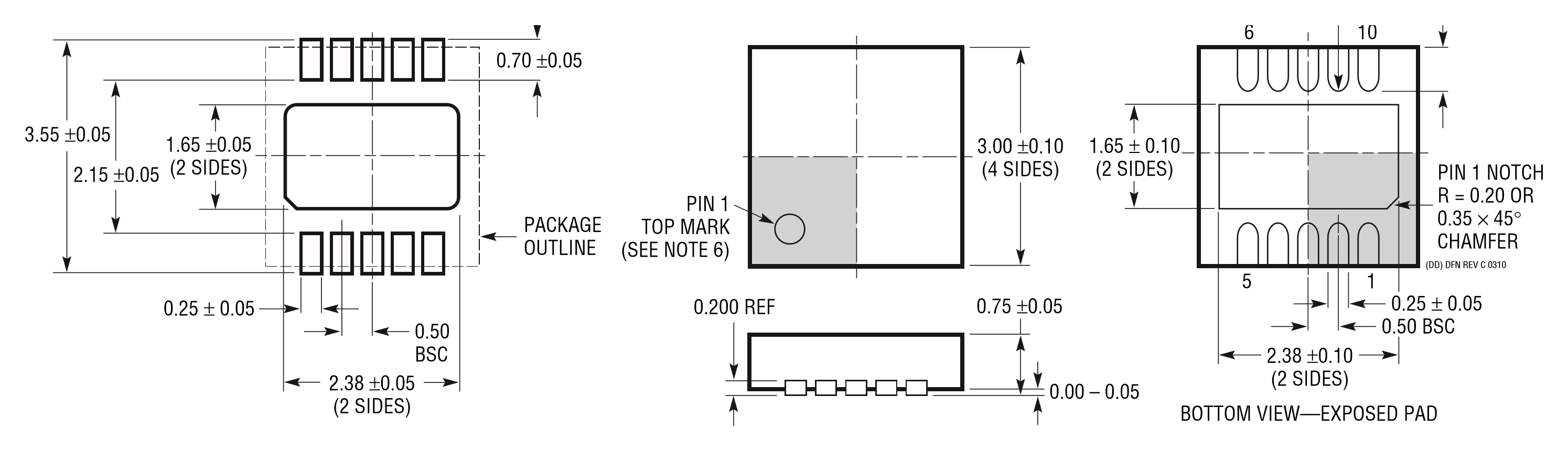
Package Information
LTC3568EDD#PBF is supplied in the 10-lead DFN (3 mm x 3 mm, DD) with exposed pad; "#PBF" marks the RoHS-compliant lead-free finish. The exposed pad on the bottom is the GND connection and the main thermal path - it must be soldered to a board copper pour with thermal vias. Keep the SW node and input capacitor loop tight, separate SGND and PGND returns and join them at the pad, and place the feedback divider close to VFB. Package dimensions and pin-1 orientation are shown below.
📄 Full specifications are detailed in the official ADI/Linear LTC3568 datasheet.
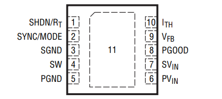
Pin Configuration
The 10-lead DFN brings out the power, switching and control pins, plus the exposed pad:
- Pin 1 - SHDN/RT: Shutdown / frequency-set resistor.
- Pin 2 - SYNC/MODE: Sync input / mode select (Burst / pulse-skip / forced-continuous).
- Pin 3 - SGND: Signal ground.
- Pin 4 - SW: Switch node (to the inductor).
- Pin 5 - PGND: Power ground.
- Pin 6 - PVIN: Power input voltage.
- Pin 7 - SVIN: Signal input voltage.
- Pin 8 - PGOOD: Power-good open-drain output.
- Pin 9 - VFB: Feedback input (0.8 V reference, R1/R2 divider).
- Pin 10 - ITH: Error-amplifier output / loop compensation.
- EP - Exposed Pad: GND and thermal path, must be soldered.
Pin 1 is marked below; the exposed pad (EP) is the center pad.
Alternative and Related Parts
The parts below are related ADI/Linear synchronous step-down regulators in our catalog. They are not all drop-in replacements; verify input range, current, frequency and pinout before substituting.
| Part Number | Brand | Type / Key Difference | Package | Note |
|---|---|---|---|---|
| LTC3548A | ADI/Linear | Dual 800mA/400mA sync buck | 10-DFN/MSOP | Dual output, lower current |
| LTC3406A | ADI/Linear | 600mA 1.5MHz sync buck | ThinSOT | Lower current, fixed/adj |
| LTC3411A | ADI/Linear | 1.25A 4MHz sync buck | 10-DFN/MSOP | Similar, lower current |
| LTC3414 | ADI/Linear | 4A 4MHz sync buck | TSSOP-EP | Higher current |
Selection Tips: Use the LTC3568 for a single 1.8 A, up-to-4 MHz synchronous buck from a 2.5-5.5 V rail. The LTC3411A is a similar 1.25 A part, the LTC3414 a higher-current 4 A part, the LTC3548A a dual-output version, and the LTC3406A a lower-current 600 mA buck in ThinSOT.
Manufacturer Information
Linear Technology, now part of Analog Devices, is known for high-performance power management. The LTC3568 is a compact high-frequency synchronous buck that integrates both power MOSFETs, delivering high efficiency in a small 3x3 mm DFN for portable rails.
The device is backed by full datasheet characterization and application notes on frequency selection, mode configuration, feedback design and grounding/thermal layout of the exposed pad - the details that determine an efficient, low-noise portable supply.
Applications


Frequently Asked Questions
What does the LTC3568EDD#PBF do?
It is a 1.8 A synchronous step-down (buck) DC/DC converter: it converts a 2.5-5.5 V input to a regulated output (0.8-5 V, adjustable), with a resistor-set 0.85-4 MHz frequency, synchronous rectification up to ~96% efficiency, in a 10-lead 3x3 mm DFN with exposed pad.
Does it have an I2C interface?
No. The output is set by an external R1/R2 resistor divider to the VFB pin (0.8 V reference), not by I2C. The SYNC/MODE pin selects operating mode and external clock sync.
How is the switching frequency set?
By an external resistor on the SHDN/RT pin, programmable from 0.85 MHz to 4 MHz. Higher frequency allows smaller inductor and capacitors.
What input voltage does it use?
2.5 V to 5.5 V, ideal for single-cell Li-ion and 3.3 V/5 V rails, delivering up to 1.8 A output.
Disclaimer
Information Accuracy: The specifications on this page are based on the official ADI/Linear LTC3568 datasheet. We work to keep the information accurate and complete, but parameters can change with product revisions, so design engineers should verify all values against the latest official documentation before final design.
Product Authenticity Guarantee: All parts we supply are genuine factory originals with full material traceability.
Technical Support: Pre-sales and post-sales technical consultation is available free of charge.
Application Notice: This page is for reference only. Suitability for a specific application should be confirmed by the design engineer against the actual system requirements.
LTC3568EDD#PBF Specifications
- Specifications
- Attributes
- Property Value
- Manufacturer
- Analog Devices Inc.
- Series:
- -
- Package/Case:
- 10-WFDFN Exposed Pad
- Packaging:
- Tube
- Part Status:
- Active
- Function:
- Step-Down
- Output Configuration:
- Positive
- Output Type:
- Adjustable
- Number of Outputs:
- 1
- Voltage - Input (Min):
- 2.25V
- Mounting Style:
- Surface Mount
- Voltage - Input (Max):
- 5.5V
- Voltage - Output (Min/Fixed):
- 0.8V
- Topology:
- Buck
- Voltage - Output (Max):
- 5V
- Current - Output:
- 1.8A
- Qualification:
- -
- Frequency - Switching:
- Up to 4MHz
- Supplier Device Package:
- 10-DFN (3x3)
- Grade:
- -
- Synchronous Rectifier:
- Yes
- Operating Temperature:
- -40°C ~ 125°C (TJ)
LTC3568EDD#PBF Relevant information
- LTC3568EDD#PBF Tags
- Popular Search
The following parts are popular search parts in Voltage Regulators - DC DC Switching Regulators.
The Posts
-
Exploring the Features of AN431AN - ATRG1 Voltage Reference IC
The AN431AN - ATRG1 is a significant voltage reference integrated circuit (IC) that plays a crucial role in maintaining stable voltage levels within electronic circuits. Engineered with precision, it o…
-
Unveiling the Wonders of XP1002000 - 05R Electronic Component
The XP1002000 - 05R is an electronic component that stands out for its specialized design and functionality, catering to a variety of electronic system requirements.Unique FeaturesOne of the most notab…
-
Unraveling the Wonders of MMBF170LT1 Transistor
The MMBF170LT1 is a remarkable transistor that has carved a niche for itself in the electronic component landscape. This tiny yet powerful device is engineered with precision to deliver outstanding per…
-
Unveiling the Marvels of MMBF170LT3G Transistor
The MMBF170LT3G is a high - performance transistor that stands out in the realm of electronic components. Engineered with precision, it brings a set of features that make it a valuable asset in numerou…
-
Unveiling the Features of RD16E - T1 - AZ Electronic Component
The RD16E - T1 - AZ is an electronic component that brings a set of unique features to the table. Its design showcases precision engineering, catering to specific requirements in various electronic set…
-
Unveiling the Capabilities of RD16ES - T1 - AZ Electronic Component
The RD16ES - T1 - AZ is a remarkable electronic component that combines advanced technology with practical design to meet the demands of diverse electronic projects.Electrical FeaturesOne of the key as…
Related Products
-
FAN53601AUC105X
onsemi
-
MIC23250-SKYMT-TR
Microchip Technology
-
TPS63002DRCTG4
Texas Instruments
-
AP1604AWG-7
Diodes Incorporated
-
FAN48617UC50X
onsemi
-
FAN48610BUC33X
onsemi
-
FAN48611UC53X
onsemi
-
FAN48615UC11X
onsemi
-
BM2P093
Rohm Semiconductor
-
MPQ2178AGQHE-AEC1-Z
Monolithic Power Systems Inc.
-
TPS61010DRCR
Texas Instruments
-
TPS61013DGSR
Texas Instruments