The Bandwidth Bottleneck Feeding Camera Data into an Accelerator
How camera data reaches an AI accelerator through pixel rate, MIPI lanes, memory traffic, preprocessing, buffering, layout and substitution review.
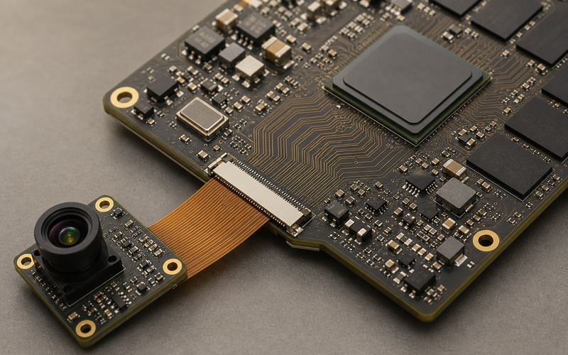
A live camera stream can overwhelm an edge AI board before inference begins. The sensor may promise a clean resolution and frame rate, while the product drops frames, adds delay or lowers the camera mode because the route after the sensor is too narrow. The limiting point may sit at the camera interface, the memory bus, the image signal processor, a resize step or the software path that passes tensors to the accelerator.
The mistake is to judge each device alone. A MIPI CSI-2 receiver may meet its lane rate, the accelerator may advertise strong operations per second and the memory device may have ample capacity. The board can still miss the target when raw pixels, converted frames, temporary buffers and model input tensors all fight for the same transfer budget.
A useful review follows the bytes from sensor output to the first tensor consumed by the accelerator. Pixel format, lane count, clocking, DMA behavior, memory width, ISP settings, crop strategy, scaling, color conversion and accelerator input format need to be approved as one path.
The Bottleneck Starts Before the Model
Inference speed is only one section of the timing chain. The product also exposes the frame, reads the sensor, transfers data across the camera link, writes memory, applies ISP work, resizes or crops, changes color format and finally feeds the prepared tensor into the accelerator.
If the path is late, the model starts late. A faster accelerator cannot recover a frame already delayed or dropped upstream. This explains why a design may benchmark well with stored images and then struggle with a live sensor.
Separate compute speed from camera data speed. Compute speed says how fast prepared tensors run. Camera data speed says how fast the board can turn live pixels into those tensors while display, network, CPU and storage activity are also present.
Begin With Pixel Rate
The first calculation is the sensor output rate. Resolution, frame rate and bits per pixel decide the raw stream before packing, compression or cropping. A 1920 by 1080 stream at 60 frames per second is a different design problem from a 640 by 480 stream at 15 frames per second, even when the final model input is a small square image.
Pixel format changes the load. RAW10, RAW12, YUV422, RGB888 and compressed streams move different amounts of data. Embedded lines, metadata, blanking and protocol overhead also use link time. A link budget that counts active pixels alone can look cleaner than the system will behave.
Use the mode the product ships. HDR, binning, high dynamic range readout, rolling shutter timing and auto exposure can change the frame cadence. The approval file should show the shipped stream rather than a friendly demo mode.
A short calculation helps purchasing and engineering discuss the same limit: active pixels times frame rate times bits per pixel, adjusted for packing and overhead. The number makes hidden movement visible.
Interface Lanes Are One Gate
MIPI CSI-2 lane speed is often checked first, but it is only one gate. The sensor, connector, flex cable, receiver PHY, SoC port and board routing need matching lane count and signal margin. A sensor mode can fit the data sheet while the receiving processor supports a lower practical mode.
Lane count affects board design and sourcing. More lanes need more connector pins, matched routing and skew control. Fewer lanes simplify routing but may force lower frame rate, lower bit depth or a different crop. The right choice comes from the real frame stream and the receiver margin.
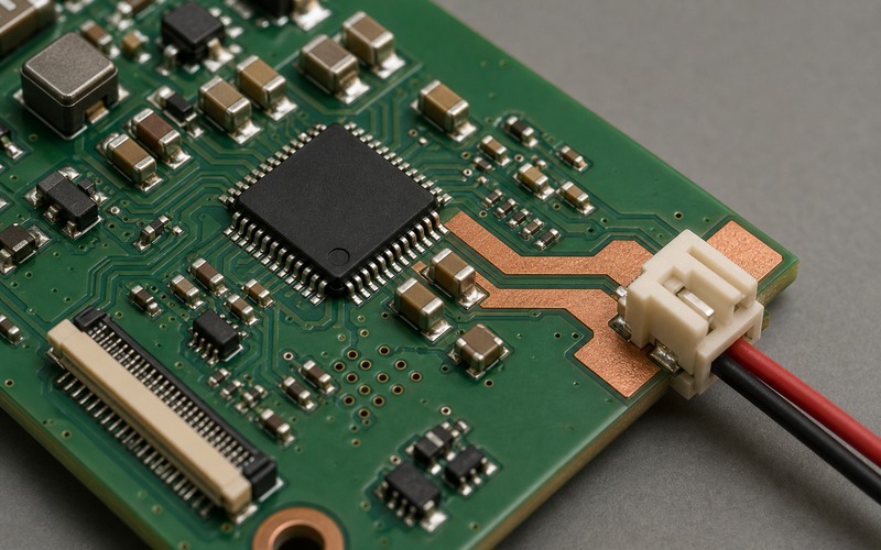
The flex cable and connector are high speed parts. Cable length, impedance, shield strategy, bend radius and insertion direction all matter. The connector should face the board edge so the FPC can leave cleanly instead of folding across the PCB.
Validation can use receiver error counters, stress patterns or eye-margin tools when available. A link that barely passes on the bench can fail after temperature, cable tolerance and enclosure routing are added.
Memory Traffic Can Exceed the Sensor Stream
A camera frame rarely moves once. The receiver may write it to memory, the ISP may read it, the scaler may write another frame, color conversion may read and write again, and the accelerator input step may pack another tensor. The memory traffic can exceed the raw sensor stream by several passes.
Memory capacity does not prove memory bandwidth. A board can have enough gigabytes and still stall on bus width, memory speed, arbitration or cache behavior. The accelerator, CPU, ISP, display engine and network interface may request memory in the same window.
The memory review should count how many blocks touch each frame and how many full-frame passes happen before inference. Cropping early can save bandwidth. Scaling late can waste it. A hardware pipeline can avoid copies, while a CPU path can add reads, writes and cache maintenance.
Several small cameras can create more pressure than one large camera because their frames arrive with separate timing and buffer needs. The system budget should cover the shipped combination, not a single quiet stream.
Preprocessing Is Part of the Link
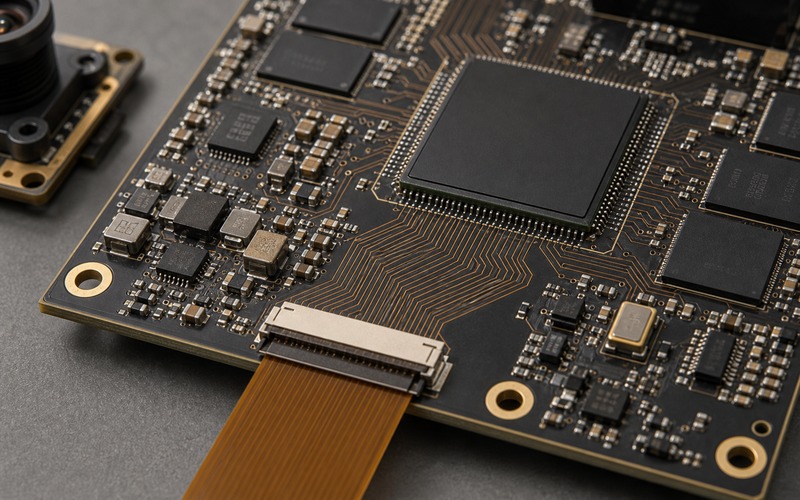
The accelerator usually expects a fixed tensor size, color order and numeric format. The camera may output a Bayer pattern, YUV stream, different bit depth or a larger frame. The conversion work between those formats is part of the data path.
Demosaic, denoise, lens correction, color conversion, crop, resize, normalization and quantization all move data. Some steps run in an ISP or hardware scaler. Some fall to CPU or GPU code. That placement decides delay, memory traffic and thermal load.
If training uses RGB input, the device should state where RGB is produced. If training uses cropped objects, the device should state whether crop happens before or after full-frame memory writes. If the accelerator uses INT8 tensors, the quantization point and buffer ownership should be clear.
Record preprocessing order, block ownership and buffer count in the approval file. Without that record, a sensor or processor substitution can change the path while the model file appears unchanged.
Buffers, DMA and Latency Need a Budget
Buffers protect the system from timing variation, but each buffer consumes memory and adds age to the frame. Too few buffers drop frames when inference stalls. Too many buffers let the product act on old images.
DMA can keep the CPU away from pixel copies, but DMA setup, alignment, cache rules and interrupts still matter. A poorly aligned buffer can turn a hardware path into a copy path. A missed cache rule can create stale frames or extra flushing.
Latency should be measured from exposure start to model output. For motion control, presence detection, sorting or safety alerts, the age of the frame is part of the decision. A high frame rate gives little value if the output is based on an old frame.
The timing budget should list exposure, sensor readout, interface transfer, memory write, preprocessing, tensor transfer, inference and postprocessing. That list shows whether the fix is a faster part, a different data route or a lower camera mode.
Multi-Camera Designs Raise the Load
Two or more cameras add synchronization, routing and memory pressure. The board may need several CSI ports, an aggregator, a switch, a deserializer or a processor with enough camera inputs. Each option changes delay and failure modes.
If frames must be compared, timestamp accuracy matters. Stereo depth, surround view and people counting across views can fail when cameras arrive at different times. Buffer depth can hide link jitter, but it also increases frame age.
Multi-camera systems also raise power and heat. Sensors, receivers, memory and accelerator load can rise together. A board that handles one camera cleanly may throttle or drop links after a second or third stream is enabled.
Validation should run all cameras at the shipped mode. Testing one camera at a time does not prove the shared memory and accelerator path.
Power and Layout Keep the Data Moving
High speed camera links are sensitive to supply noise, reference clock quality, return paths and impedance control. A regulator that works for ordinary digital logic can still add jitter or receiver errors if it is placed poorly near the PHY or clock.
Route matched lanes with controlled impedance, clean return paths and spacing from noisy switching nodes. Keep the connector orientation friendly to assembly and cable strain. Use local decoupling near the receiver, accelerator and memory packages.
The accelerator and memory can draw burst current while frames arrive. If voltage droop hits during a camera transfer, the failure may look like a protocol issue. Power, clock and signal checks should be reviewed together.
Thermal behavior belongs in the same check. A hot accelerator can throttle, a warm memory device can lose margin and a cable near a heat source can age faster. Run live camera mode while checking temperature and link errors.
Substitution Review for the Data Path
A substitute image sensor can change pixel packing, lane count, frame timing and embedded metadata. A substitute connector or flex can change impedance and insertion direction. A substitute processor can change receiver limits, memory architecture or accelerator input format. These are data-path changes.
Second sourcing should start from the shipped stream. If a new sensor mode needs more lanes, if a new accelerator needs a different tensor layout or if a memory package changes bandwidth, the model may need new validation even when the outline stays close.
The approval file should mark which substitutions are safe without firmware change, which need firmware work and which require model validation. Procurement then has a clear action path rather than a loose compatibility note.
Tie exact orderable identifiers to the tested mode. Camera module suffix, connector height, processor speed grade and memory width can all matter. A small ordering change can move the bottleneck.
Release Checklist
Before release, run the final camera mode through the full path. Record sensor settings, lane count, pixel format, frame rate, memory traffic estimate, preprocessing order, buffer count, accelerator input format, measured latency and link error counters if the platform exposes them.
Verify timing under field load. Run the accelerator, memory, network, display or storage path that the product uses. A quiet bench image can hide contention that appears when the finished device is busy.
The final record should state accepted stream modes, approved connectors and flex paths, allowed processor and memory variants, firmware assumptions and triggers for revalidation. Camera bandwidth is not a single number in a data sheet. It is the movement budget of the whole vision path, from sensor pins to the first tensor consumed by the accelerator.