- Products
- Marking
- Alternative
Texas Instruments 1P1G125QDRYRQ1

- Part No.:
- 1P1G125QDRYRQ1
- Manufacturer:
- Texas Instruments
- Package:
- 6-UFDFN
- Datasheet:
-
 1P1G125QDRYRQ1.pdf
- Description:
- IC BUFFER NON-INVERT 5.5V 6SON
- Quantity:
Unit Price:$0.000000
Ext Price:$0.000000
- Payment:

- Shipping:

Inventory:2,571
Send us your inquiry,we will respond immediately.
In Stock : 2,571 PCS
| Qty. | Unit Price | Ext Price |
| 0+ | $0.000000 | $0.000000 |
*Products eligible for online ordering ship within 1-2 business days,please contact us for exact shipping times.
Also you can RFQ for 1P1G125QDRYRQ1 or email to us: Email: [email protected] , we will contact you within 12 hours.
Product Details
1P1G125QDRYRQ1 (Texas Instruments SN74LVC1G125-Q1) - 3-State Bus Buffer in Tiny SON (DRY) Package, Active-Low OE
1P1G125QDRYRQ1 is the InFortune ordering code for the Texas Instruments SN74LVC1G125-Q1 single 3-state bus buffer in its smallest body: the DRY package, a 6-pin SON measuring about 1.45 mm × 1.00 mm at 0.55 mm height. It delivers the full LVC buffer — active-low 3-state output (Y = A / Hi-Z), 1.65 V to 5.5 V, 5.5 V-tolerant inputs, ±24 mA drive, Ioff and AEC-Q100 automotive qualification — in a footprint chosen when board area is the hard constraint, such as wearables, hearables and dense portable boards.
Product Introduction
The SN74LVC1G125-Q1 is a single 3-state bus buffer: the output follows the input (Y = A) when the active-low output-enable is asserted and goes high-impedance otherwise, so the device can drive or release a shared line. This order option packs that function into the DRY (SON) outline — one of the smallest standard packages able to carry a complete single gate — for designs where every square millimetre counts.
Despite the size, nothing is given up electrically. The inputs are 5.5 V-tolerant and the output swings to VCC, so the part still does clean down-translation (read a 5 V signal, present it at a 3.3 V or 1.8 V rail) with a strong ±24 mA drive. The Ioff partial-power-down circuit still supports live insertion and back-drive protection, and the “-Q1” automotive qualification (−40 °C to +125 °C) still applies.
The DRY package is a 6-pin SON: the five buffer signals plus one no-connect (NC) pin. At about 10 µA quiescent it suits battery-powered wearables, hearables, medical sensors and other space- and power-constrained boards that still need a clean, isolatable bus interface.
Expert Technical Insight
Choosing the SON (DRY) outline for a single-gate buffer:
- Smallest area, but mind the assembly: the leadless SON at 0.55 mm height saves board area and z-height versus SC-70/SOT-23, but its bottom-terminated pads need a controlled stencil and reflow profile — plan the land pattern from the package drawing, not a generic footprint.
- The NC pin is not a tie-point: pin 5 on the 6-pin SON is a true no-connect; leave it floating or to an isolated pad — do not use it as a via or tie it to a rail.
- Full function in a tiny body: down-translation, Ioff live-insertion and ±24 mA drive are all retained, so the SON choice is purely about space — you are not trading away the buffer’s electrical capability.
Key Benefits
~1.45 mm × 1.00 mm, 0.55 mm height — among the smallest bodies for a full single-gate buffer, ideal for wearables and dense boards.
Inputs accept 5.5 V at any VCC; output swings to VCC for clean 5 V→3.3 V/1.8 V translation with ±24 mA drive.
Active-low 3-state output for bus sharing; Ioff supports live insertion and back-drive protection even in this small package.
AEC-Q100 Grade 1 (−40 °C to +125 °C) at about 10 µA quiescent for portable and in-vehicle sensors.
Specifications
| Parameter | Value | Conditions / Notes |
|---|---|---|
| Device Type | Single 3-state bus buffer / line driver | One channel; LVC family |
| Manufacturer | Texas Instruments | SN74LVC1G125-Q1 (data sheet SGES002E) |
| Logic Function | Y = A when OE = L; Hi-Z when OE = H | Active-LOW output enable |
| Automotive Qualification | AEC-Q100 Grade 1 (−40 °C to +125 °C) | HBM Level 2, CDM Level C5 |
| Supply Voltage (VCC) | 1.65 V to 5.5 V | Data retention down to 1.5 V |
| Input Tolerance | Up to 5.5 V | A and OE accept voltages above VCC |
| Output Drive (IOH/IOL) | ±24 mA at 3.3 V | Down to ±4 mA at 1.65 V |
| Propagation Delay (tpd) | 5.1 ns max at 3.3 V | 4.1 ns max at 5 V |
| Enable / Disable Time | ten 6.0 ns / tdis 5.0 ns max | OE→Y at 3.3 V |
| Ioff (partial power down) | ±10 µA max | Live insertion / back-drive protection |
| Quiescent Current (ICC) | 10 µA max | Full VCC range |
| Input Capacitance (Ci) | 4 pF max | VCC = 3.3 V |
| ESD (HBM / CDM) | ±2000 V / ±1000 V | AEC Q100-002 / Q100-011 |
| Operating Temperature (TA) | −40 °C to +125 °C | Grade 1 |
| Package | 6-pin SON (DRY) | ≈ 1.45 mm × 1.00 mm, 0.55 mm height; 1 NC pin |
Note: Values are from the Texas Instruments SN74LVC1G125-Q1 data sheet (SGES002E). Confirm every parameter against the latest data sheet before committing a design.
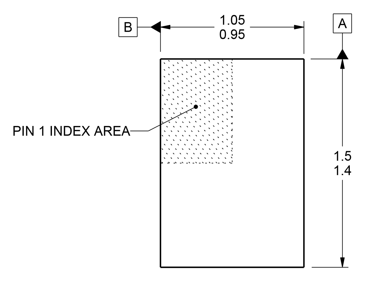
Package Information
This order option uses the DRY package — a 6-pin SON (leadless), about 1.45 mm × 1.00 mm with a 0.55 mm maximum height and 0.5 mm pitch. It is one of the smallest outlines available for a complete single-gate buffer, trading the easy-to-inspect leads of SC-70/SOT-23 for minimum board area and z-height. The same die is also offered in DCK (SC-70) and DBV (SOT-23) for less space-critical designs.
Use the dimensioned drawing below to build the SON land pattern, paste stencil and keep-out — bottom-terminated parts are sensitive to footprint and reflow.
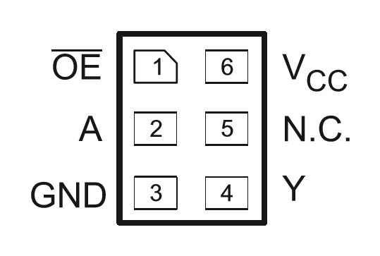
Pin Configuration (6-Pin SON)
The DRY package adds one no-connect to the five buffer signals (top view):
- Pin 1 – OE (Output Enable, active-low): low enables Y = A; high forces Hi-Z. 5.5 V-tolerant.
- Pin 2 – A (Input): data input; 5.5 V-tolerant.
- Pin 3 – GND: Ground (0 V) reference.
- Pin 4 – Y (Output): 3-state output; ±24 mA at 3.3 V or Hi-Z.
- Pin 5 – NC: No internal connection; leave floating (do not use as a tie-point or via).
- Pin 6 – VCC: Supply, 1.65 V to 5.5 V; decouple with a local 0.1 µF capacitor.
Alternative Parts
The same buffer in larger packages, plus family alternatives. The first row is the SC-70 option of this device; the SN74LVC1G126 is the active-high counterpart. Confirm package, family and enable polarity before substituting.
| Part Number | Brand | Function | Package | Note |
|---|---|---|---|---|
| 1P1G125QDCKRG4Q1 | Texas Instruments | 3-state buffer, active-LOW OE | SC-70-5 | Same device, easier-to-assemble SC-70 |
| SN74LVC1G125DBVR | Texas Instruments | 3-state buffer, active-LOW OE | SOT-23-5 | Same gate, SOT-23 package option |
| SN74LVC1G126DBVR | Texas Instruments | 3-state buffer, active-HIGH OE | SOT-23-5 | Complementary enable polarity |
| SN74AUP1G125DCKR | Texas Instruments | 3-state buffer, active-LOW OE | SC-70-5 | Ultra-low-power AUP for battery designs |
Logic Family Comparison
| Family | Supply Range | Position | Use When |
|---|---|---|---|
| LVC-Q1 (this part) | 1.65–5.5 V | Wide-supply, 5 V-tolerant, automotive | Space-critical mixed-voltage buses |
| AHC | 2–5.5 V | General-purpose | Standard 5 V/3.3 V buffering |
| AUP | 0.8–3.6 V | Ultra-low-power | Battery / wearable |
| AUC | 0.8–2.7 V | Very high speed | Sub-2 V core logic |
Manufacturer Information
Texas Instruments (TI, NASDAQ: TXN), of Dallas, Texas, offers its single-gate logic in a wide range of packages from SOT-23 down to leadless SON/X2SON, so designers can keep the same proven LVC die while optimising for board area. The “-Q1” variants are AEC-Q100 qualified.
The governing document is the SN74LVC1G125-Q1 data sheet (SGES002E), which defines the electrical limits, the Ioff behaviour and the DRY/DCK/DBV package outlines. InFortune Electronics supplies the device under code 1P1G125QDRYRQ1 and provides sourcing and technical support.
Application Areas


Frequently Asked Questions (FAQ)
How big is the DRY (SON) package?
About 1.45 mm × 1.00 mm with a 0.55 mm maximum height — a 6-pin leadless SON, one of the smallest outlines for a full single-gate buffer. The same die is also available in SC-70 (DCK) and SOT-23 (DBV).
Why does this package have 6 pins when the buffer needs 5?
The SON outline adds one no-connect (NC) pin (pin 5); the five signals are OE, A, GND, Y and VCC. Leave the NC pin floating — do not use it as a tie-point or via.
Does the small package reduce the electrical performance?
No. It is the same SN74LVC1G125-Q1 die: 1.65–5.5 V, 5.5 V-tolerant inputs, ±24 mA drive, Ioff and AEC-Q100 grade are all retained. The SON choice is purely about board area.
Is the output enable active-low?
Yes — the SN74LVC1G125 drives Y = A when OE is low and is Hi-Z when OE is high. For an active-high enable, use the SN74LVC1G126.
Disclaimer
Information Accuracy: Technical specifications on this page are based on the Texas Instruments SN74LVC1G125-Q1 data sheet (SGES002E). We strive for accuracy and completeness, but specifications are subject to change without notice.
Product Authenticity: We guarantee all products are genuine factory originals with complete material traceability.
Technical Support: Free technical consultation is available before and after purchase.
Application Note: This product page is for reference only. Suitability for a specific application should be verified by design engineers against actual system requirements.
1P1G125QDRYRQ1 Specifications
- Specifications
- Attributes
- Property Value
- Manufacturer
- Texas Instruments
- Series:
- 74LVC
- Package/Case:
- 6-UFDFN
- Packaging:
- Tape & Reel (TR)
- Part Status:
- Active
- Logic Type:
- Buffer, Non-Inverting
- Number of Elements:
- 1
- Input Type:
- -
- Output Type:
- 3-State
- Current - Output High, Low:
- 24mA, 24mA
- Voltage - Supply:
- 1.65V ~ 5.5V
- Operating Temperature:
- -40°C ~ 125°C (TA)
- Number of Bits per Element:
- 1
- Grade:
- Automotive
- Qualification:
- AEC-Q100
- Mounting Style:
- Surface Mount
- Supplier Device Package:
- 6-SON (1.45x1)
1P1G125QDRYRQ1 Relevant information
- 1P1G125QDRYRQ1 Tags
- Popular Search
The following parts are popular search parts in Buffers, Drivers, Receivers, Transceivers.
The Posts
-
0473003.YRT1L LITTELFUSE Fuse: Applications, Selection Guide, Alternatives and Buying Notes
0473003.YRT1L LITTELFUSE guide for 3 A PICO II 473 slow-blow axial fuse use, 125 V ratings, alternatives and sourcing checks.

-
0451005.MR LITTELFUSE Fuse: Applications, Selection Guide, Alternatives and Buying Notes
0451005.MR LITTELFUSE fuse guide for 5 A NANO2 451 use, obsolete-status review, alternatives, replacement risk and sourcing checks.
-
0251.062NRT1L LITTELFUSE Fuse: Applications, Selection Guide, Alternatives and Buying Notes
0251.062NRT1L LITTELFUSE fuse guide for 62 mA PICO II 251 use, 125 V rating, axial PCB fit and sourcing checks.
-
0251001.NRT1L LITTELFUSE Fuse: Applications, Selection Guide, Alternatives and Buying Notes
0251001.NRT1L LITTELFUSE guide for 1 A PICO II 251 axial fuse use, 125 V ratings, PCB fit, alternatives and sourcing checks.
-
0154001.DR LITTELFUSE Fuse: Applications, Selection Guide, Alternatives and Buying Notes
0154001.DR LITTELFUSE fuse guide for 1 A OMNI-BLOK 154 use, 125 V rating, PCB footprint review, alternatives and sourcing checks.
-
0154.062DR LITTELFUSE Fuse: Applications, Selection Guide, Alternatives and Buying Notes
0154.062DR LITTELFUSE fuse guide covering 62 mA OMNI-BLOK use, 125 V ratings, PCB holder fit, alternatives and sourcing checks.
-
XH414HG-IV01E SEIKO EDLC: Applications, Selection Guide and Buying Notes
XH414HG-IV01E SEIKO EDLC guide for 3.3V RTC backup, IV01E pinout and terminal checks, alternatives, replacement risk and sourcing review for buyers before RFQ.
-
XH414HG-II06E SEIKO EDLC: Applications, Selection Guide and Buying Notes
XH414HG-II06E SEIKO EDLC guide covering RTC backup use, 3.3V charging, opposite-side pinout and terminals, alternatives, replacement risk and sourcing checks.
Related Products
-
CD74FCT2244ATM
Harris Corporation
-
DM74S244N
Fairchild Semiconductor
-
SN74LVTH543DW
Texas Instruments
-
CD74HC365MT
Texas Instruments
-
SN74LV126ANS
Texas Instruments

-
SN74LVTH540DW
Texas Instruments
-
CD74HC365M
Texas Instruments
-
CD74HCT240PW
Texas Instruments
-
CD74HCT240PWT
Texas Instruments
-
74VCX162244MTD
onsemi
-
CD74AC244M
Texas Instruments
-
SN74ALVC126D
Texas Instruments