- Products
- Marking
- Alternative
Texas Instruments 1P1G126QDRYRQ1

- Part No.:
- 1P1G126QDRYRQ1
- Manufacturer:
- Texas Instruments
- Package:
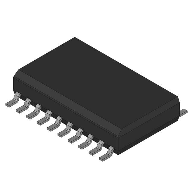
- 6-UFDFN
- Datasheet:
-
 1P1G126QDRYRQ1.pdf
- Description:
- IC BUFFER NON-INVERT 5.5V 6SON
- Quantity:
Unit Price:$0.000000
Ext Price:$0.000000
- Payment:

- Shipping:

Inventory:2,097
Send us your inquiry,we will respond immediately.
In Stock : 2,097 PCS
| Qty. | Unit Price | Ext Price |
| 0+ | $0.000000 | $0.000000 |
*Products eligible for online ordering ship within 1-2 business days,please contact us for exact shipping times.
Also you can RFQ for 1P1G126QDRYRQ1 or email to us: Email: [email protected] , we will contact you within 12 hours.
Product Details
1P1G126QDRYRQ1 (Texas Instruments SN74LVC1G126-Q1) - Active-High 3-State Bus Buffer in Tiny SON (DRY) Package
1P1G126QDRYRQ1 is the InFortune ordering code for the Texas Instruments SN74LVC1G126-Q1 single 3-state bus buffer with an active-HIGH output enable, supplied in the smallest body: the DRY 6-pin SON (~1.45 mm × 1.00 mm, 0.55 mm height). It drives Y = A when the enable is high and is high-impedance when low, runs from 1.65 V to 5.5 V with 5.5 V-tolerant inputs, delivers ±24 mA, and supports Ioff live insertion — the full automotive (-Q1) buffer in a footprint chosen when board area is the constraint.
Product Introduction
The SN74LVC1G126-Q1 is a single 3-state bus buffer with an active-HIGH output enable: the output follows the input (Y = A) when OE is high and switches to high-impedance when OE is low. This order option delivers that function in the DRY (SON) package — a 6-pin leadless outline among the smallest that can carry a complete single gate — for area-critical boards that still need clean, gated bus access with high-true enable logic.
Nothing is sacrificed electrically. Inputs are 5.5 V-tolerant and the output swings to VCC, so the part performs clean down-translation with a strong ±24 mA drive, and the Ioff partial-power-down circuit still supports live insertion and back-drive protection. The “-Q1” automotive qualification (−40 °C to +125 °C) applies, at about 10 µA quiescent.
The active-high enable is the only logical difference from the SN74LVC1G125 (active-low). Choosing the '126 lets a naturally high-true grant or select signal enable the buffer directly, without an inverter in the control path — useful when board area is already tight.
Expert Technical Insight
Picking the active-high buffer in the smallest package:
- Enable polarity removes glue logic: a high-true enable drives the '126 directly; using the active-low '125 in that slot would need an inverter — extra area you are trying to save by choosing SON.
- SON layout discipline: the leadless 6-pin body (one pin is NC) saves area and z-height but needs a controlled land pattern and stencil; build the footprint from the package drawing, and leave the NC pin floating.
- Same silicon, same ratings: 5.5 V tolerance, ±24 mA drive, Ioff and AEC-Q100 grade are identical to the SOT-23 option — the SON choice is purely mechanical.
Key Benefits
High-true 3-state enable in a ~1.45 mm × 1.00 mm leadless SON — full buffer where board area is the constraint.
Inputs to 5.5 V at any VCC; output to VCC for clean 5 V→3.3 V/1.8 V translation with ±24 mA drive.
Partial-power-down keeps the I/O Hi-Z while unpowered, protecting a live bus during hot insertion.
AEC-Q100 Grade 1 (−40 °C to +125 °C) at about 10 µA quiescent.
Specifications
| Parameter | Value | Conditions / Notes |
|---|---|---|
| Device Type | Single 3-state bus buffer / line driver | One channel; LVC family |
| Manufacturer | Texas Instruments | SN74LVC1G126-Q1 (data sheet SCES467D) |
| Logic Function | Y = A when OE = H; Hi-Z when OE = L | Active-HIGH output enable |
| Automotive Qualification | AEC-Q100 Grade 1 (−40 °C to +125 °C) | Qualified for automotive applications |
| Supply Voltage (VCC) | 1.65 V to 5.5 V | Data retention down to 1.5 V |
| Input Tolerance | Up to 5.5 V | A and OE accept voltages above VCC |
| Output Drive (IOH/IOL) | ±24 mA at 3.3 V | Down to ±4 mA at 1.65 V |
| Propagation Delay (tpd) | 5.8 ns max at 3.3 V | 4.5 ns max at 5 V |
| Enable / Disable Time | ten 5.8 ns / tdis 6.0 ns max | OE→Y at 3.3 V |
| Ioff (partial power down) | ±10 µA max | Live insertion / back-drive protection |
| Quiescent Current (ICC) | 10 µA max | Full VCC range |
| Input Capacitance (Ci) | 4 pF typ | VCC = 3.3 V |
| ESD (HBM / CDM) | ±2000 V / ±1000 V | AEC Q100-002 / Q100-011 |
| Operating Temperature (TA) | −40 °C to +125 °C | Grade 1 |
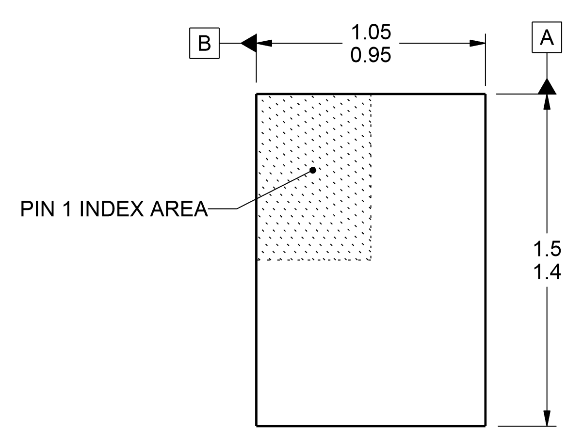
| Package | 6-pin SON (DRY) | ≈ 1.45 mm × 1.00 mm, 0.55 mm height; 1 NC pin |
Note: Values are from the Texas Instruments SN74LVC1G126-Q1 data sheet (SCES467D). Confirm every parameter against the latest data sheet before committing a design.
Package Information
This order option uses the DRY package — a 6-pin SON (leadless), about 1.45 mm × 1.00 mm with a 0.55 mm maximum height. It trades the easy-to-inspect leads of SOT-23 for minimum board area and z-height. The same active-high buffer die is also offered in DBV (SOT-23) for less space-critical designs.
Use the dimensioned drawing below to build the SON land pattern and stencil — bottom-terminated parts are sensitive to footprint and reflow.
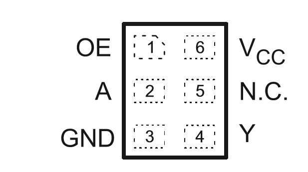
Pin Configuration (6-Pin SON)
The DRY package adds one no-connect to the five buffer signals (top view):
- Pin 1 – OE (Output Enable, active-high): high enables Y = A; low forces Hi-Z. 5.5 V-tolerant.
- Pin 2 – A (Input): data input; 5.5 V-tolerant.
- Pin 3 – GND: Ground (0 V) reference.
- Pin 4 – Y (Output): 3-state output; ±24 mA at 3.3 V or Hi-Z.
- Pin 5 – NC: No internal connection; leave floating.
- Pin 6 – VCC: Supply, 1.65 V to 5.5 V; decouple with a local 0.1 µF capacitor.
Alternative Parts
The same active-high buffer in SOT-23, plus the active-low counterpart and family options. Confirm package, family and enable polarity before substituting.
| Part Number | Brand | Function | Package | Note |
|---|---|---|---|---|
| 1P1G126QDBVRQ1 | Texas Instruments | 3-state buffer, active-HIGH OE | SOT-23-5 | Same device, easier-to-assemble SOT-23 |
| SN74LVC1G125DBVR | Texas Instruments | 3-state buffer, active-LOW OE | SOT-23-5 | Active-low counterpart |
| SN74AHC1G126DBVR | Texas Instruments | 3-state buffer, active-HIGH OE | SOT-23-5 | AHC family, 2–5.5 V |
| SN74LVC1G126DBVR | Texas Instruments | 3-state buffer, active-HIGH OE | SOT-23-5 | Commercial-grade LVC option |
Logic Family Comparison
| Family | Supply Range | Position | Use When |
|---|---|---|---|
| LVC-Q1 (this part) | 1.65–5.5 V | Wide-supply, 5 V-tolerant, automotive | Space-critical active-high bus gating |
| AHC | 2–5.5 V | General-purpose | Standard 5 V/3.3 V buffering |
| AHCT | 4.5–5.5 V | TTL-level inputs | 5 V TTL interfacing |
| AUP | 0.8–3.6 V | Ultra-low-power | Battery / portable |
Manufacturer Information
Texas Instruments (TI, NASDAQ: TXN), of Dallas, Texas, offers its single 3-state buffers in both enable polarities and a wide range of packages from SOT-23 down to leadless SON, letting designers match enable sense and board area while keeping the same proven LVC die. The “-Q1” variants are AEC-Q100 qualified.
The governing document is the SN74LVC1G126-Q1 data sheet (SCES467D), defining the 3-state behaviour, Ioff and the DBV/DRY packages. InFortune Electronics supplies the device under code 1P1G126QDRYRQ1 and provides sourcing and technical support.
Application Areas


Frequently Asked Questions (FAQ)
Is the output enable active-high?
Yes. The SN74LVC1G126 drives Y = A when OE is high and is Hi-Z when OE is low. The active-low counterpart is the SN74LVC1G125.
How big is the DRY (SON) package?
About 1.45 mm × 1.00 mm with a 0.55 mm maximum height — a 6-pin leadless SON (one NC pin). The same die is also available in SOT-23 (DBV).
Does the small package change the electrical specs?
No. It is the same SN74LVC1G126-Q1 die: 1.65–5.5 V, 5.5 V-tolerant inputs, ±24 mA drive, Ioff and AEC-Q100 grade are retained. The SON choice is purely about board area.
What is the NC pin for?
The 6-pin SON has one no-connect (pin 5); the five signals are OE, A, GND, Y and VCC. Leave the NC pin floating — do not use it as a tie-point or via.
Disclaimer
Information Accuracy: Technical specifications on this page are based on the Texas Instruments SN74LVC1G126-Q1 data sheet (SCES467D). We strive for accuracy and completeness, but specifications are subject to change without notice.
Product Authenticity: We guarantee all products are genuine factory originals with complete material traceability.
Technical Support: Free technical consultation is available before and after purchase.
Application Note: This product page is for reference only. Suitability for a specific application should be verified by design engineers against actual system requirements.
1P1G126QDRYRQ1 Specifications
- Specifications
- Attributes
- Property Value
- Manufacturer
- Texas Instruments
- Series:
- -
- Package/Case:
- 6-UFDFN
- Packaging:
- Tape & Reel (TR)
- Part Status:
- Active
- Logic Type:
- Buffer, Non-Inverting
- Number of Elements:
- 1
- Input Type:
- -
- Output Type:
- 3-State
- Current - Output High, Low:
- 32mA, 32mA
- Voltage - Supply:
- 1.65V ~ 5.5V
- Operating Temperature:
- -40°C ~ 125°C (TA)
- Number of Bits per Element:
- 1
- Grade:
- Automotive
- Qualification:
- AEC-Q100
- Mounting Style:
- Surface Mount
- Supplier Device Package:
- 6-SON (1.45x1)
1P1G126QDRYRQ1 Relevant information
- 1P1G126QDRYRQ1 Tags
- Popular Search
The following parts are popular search parts in Buffers, Drivers, Receivers, Transceivers.
The Posts
-
0473003.YRT1L LITTELFUSE Fuse: Applications, Selection Guide, Alternatives and Buying Notes
0473003.YRT1L LITTELFUSE guide for 3 A PICO II 473 slow-blow axial fuse use, 125 V ratings, alternatives and sourcing checks.

-
0451005.MR LITTELFUSE Fuse: Applications, Selection Guide, Alternatives and Buying Notes
0451005.MR LITTELFUSE fuse guide for 5 A NANO2 451 use, obsolete-status review, alternatives, replacement risk and sourcing checks.
-
0251.062NRT1L LITTELFUSE Fuse: Applications, Selection Guide, Alternatives and Buying Notes
0251.062NRT1L LITTELFUSE fuse guide for 62 mA PICO II 251 use, 125 V rating, axial PCB fit and sourcing checks.
-
0251001.NRT1L LITTELFUSE Fuse: Applications, Selection Guide, Alternatives and Buying Notes
0251001.NRT1L LITTELFUSE guide for 1 A PICO II 251 axial fuse use, 125 V ratings, PCB fit, alternatives and sourcing checks.
-
0154001.DR LITTELFUSE Fuse: Applications, Selection Guide, Alternatives and Buying Notes
0154001.DR LITTELFUSE fuse guide for 1 A OMNI-BLOK 154 use, 125 V rating, PCB footprint review, alternatives and sourcing checks.
-
0154.062DR LITTELFUSE Fuse: Applications, Selection Guide, Alternatives and Buying Notes
0154.062DR LITTELFUSE fuse guide covering 62 mA OMNI-BLOK use, 125 V ratings, PCB holder fit, alternatives and sourcing checks.
-
XH414HG-IV01E SEIKO EDLC: Applications, Selection Guide and Buying Notes
XH414HG-IV01E SEIKO EDLC guide for 3.3V RTC backup, IV01E pinout and terminal checks, alternatives, replacement risk and sourcing review for buyers before RFQ.
-
XH414HG-II06E SEIKO EDLC: Applications, Selection Guide and Buying Notes
XH414HG-II06E SEIKO EDLC guide covering RTC backup use, 3.3V charging, opposite-side pinout and terminals, alternatives, replacement risk and sourcing checks.
Related Products
-
CD74FCT2244ATM
Harris Corporation
-
DM74S244N
Fairchild Semiconductor
-
SN74LVTH543DW
Texas Instruments
-
CD74HC365MT
Texas Instruments
-
SN74LV126ANS
Texas Instruments

-
SN74LVTH540DW
Texas Instruments
-
CD74HC365M
Texas Instruments
-
CD74HCT240PW
Texas Instruments
-
CD74HCT240PWT
Texas Instruments
-
74VCX162244MTD
onsemi
-
CD74AC244M
Texas Instruments
-
SN74ALVC126D
Texas Instruments