Free Shipping Over$200

- Products
- Marking
- Alternative

Pairing Compute with Memory That Keeps It Fed
Compute is only as fast as the data reaching it. An accelerator or an MCU running a model spends much of its time reading weights and writing activations, and where those bytes live, and how quickly they arrive, sets the speed the system reaches. Memory on an edge device is not one thing. It is a small hierarchy, each tier holding a different kind of data with a different access pattern, and choosing the parts for each tier is its own piece of the design rather than an afterthought to the silicon that does the math.
The tiers divide by job. The boot image and firmware live in non-volatile storage the part reads at startup. The model weights sit wherever the compute can stream them fast enough during inference. The working activations live in fast on-chip or external RAM. Calibration and configuration, small and rarely changed, sit in a tiny store of their own. A part chosen for one of these tiers is the wrong part for another, and a design that treats memory as a single line on the schematic tends to discover the distinction late.
The slowest tier in the path sets the pace.
The bandwidth that sets the pace
The figure behind all of this is bandwidth. How memory bandwidth caps real inference speed is the longer story, and its short form sits at the centre of every choice on this page: a model runs at the rate its weights arrive, and a fast processor starved of memory bandwidth idles while it waits for the next block. The storage tiers exist to feed that rate. The part that throttles it is the one that fixes the frame count, whatever the compute behind it claims on paper, which is why sizing the memory path comes before trusting the headline number on the processor.
The reason bandwidth bites is that a neural network reads more than it computes for. Each layer pulls its full set of weights across the bus to produce one set of activations, so a model with millions of parameters moves millions of bytes per inference no matter how clever the math unit is. This ratio, the bytes moved against the operations done, is what decides whether a design is held back by its compute or by its memory, and on the typical part running a real model at the edge, it is the memory. A processor rated for high throughput on a benchmark that fits in cache can fall to a fraction of that figure once the model is large enough to live in external flash or RAM, and the gap between the two numbers is the bandwidth of the path feeding it.
Where the boot image and code live
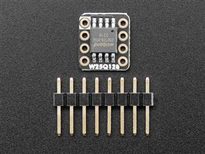
The first tier a device touches is the non-volatile store it boots from. On many edge designs this is a serial NOR flash: dense enough to hold the firmware and often the model, cheap, and simple to wire over a few pins. The part either feeds code to the processor on demand, or holds an image that is copied into RAM at startup and run from there, and which of those it does shapes both the boot time and the part that suits the job.
W25Q128JV holding the boot image and model on an edge device is a common choice for that tier, a 128-megabit SPI NOR with the density to carry a firmware image and a quantised model side by side, leaving the processor to copy the model into working memory before the first inference. The copy is not free: a large model read out of a serial flash at boot adds a visible delay to power-on, and on a device that wakes, infers, and sleeps to save a battery, that delay is part of the energy budget rather than a one-time cost. IS25LP128 as code storage for edge AI sits in the same tier with the emphasis on holding code, a pin-compatible-class SPI NOR that a design can lean on for execute-in-place or for the firmware image, and having a second source of this kind in the same density is the difference between a shortage being an inconvenience and being a redesign. The interface matters as much as the capacity. A boot image read over a single SPI line returns slowly enough that a large model adds seconds to power-on, while the same part read in quad mode cuts that to a fraction, so the pin count the design can spare for the flash feeds straight back into how long the user waits at switch-on. Density and speed trade against package and temperature as well: a part in a small package for a dense board may not carry the grade rating a larger one does, and a flash that holds its image on the bench can lose retention at the top of an industrial range, so the operating environment sits in this choice beside the megabit count. Both parts answer the same question in the end: how much has to survive a power cycle, and how fast does it have to be back when the power returns. Getting the density right with headroom for a firmware that grows over the product's life, and getting the read speed right for the boot time the product can tolerate, is the work this tier asks for, and it is the kind of work that looks trivial on the schematic and turns expensive once the part is already placed and the image no longer fits.
The temptation is to size this store for today's image. The firmware on a shipped product grows with every update, so the part that fit at launch can run out of room two years in, and the cheap time to add headroom is while the board is still on the bench.
How the code runs out of this tier is its own decision. A part that executes in place feeds instructions to the processor straight from the flash, saving the RAM a copy would need but tying execution speed to the flash interface; a part that holds a compressed image hands it to RAM once at boot and runs fast afterwards at the cost of the copy time and the RAM to land in. Many edge designs do some of both, running the hot path from RAM and leaving cold code in flash, and naming which is which early keeps the RAM budget honest.
Reliability lives here too. A device that updates itself in the field needs the boot store to survive a power cut in the middle of a write, which usually means holding two images and falling back to the known-good one if the new image fails to verify. That redundancy doubles the space the tier has to provide, and a design that leaves it out finds the need the first time an update bricks a unit in the field rather than on the bench.
Streaming weights fast enough
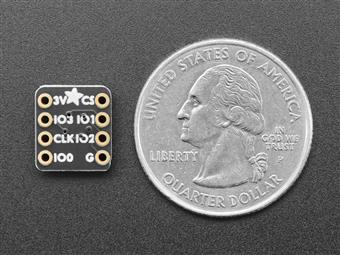
Holding the model is one job; feeding it to the compute fast enough is another, and it is where bandwidth stops being abstract. A model read one bit at a time over plain SPI starves a capable accelerator. MT25QL128 feeding weights over QSPI answers that with a quad or higher-width serial interface, multiplying the bytes per clock so the weights arrive at a rate the compute can use rather than wait on.
The choice here is driven by the gap between how fast the part can read and how fast the model needs its weights. A small model that fits on-chip never touches this tier; a larger one streamed from external flash lives or dies by it. Matching the interface width and clock to the model's demand, rather than to a number on the data sheet, is what keeps the accelerator busy instead of stalled.
On-chip memory changes the sum. A part with enough internal SRAM to hold the working set reads each weight once and keeps the activations close, so the external tier only carries the initial load; a part short of it spills to external RAM mid-inference and pays the bandwidth penalty on every layer. The size of that internal memory, not the clock on the core, is often what separates a part that hits its frame rate from one that does not, and it is the figure to check before the throughput claim is taken at face value.
When a single serial part cannot keep up, the path widens. An octal-interface flash, a part that streams from two dies at once, or a higher-bandwidth memory such as HyperRAM sitting between the flash and the compute, each buys more bytes per clock at the cost of pins, board area, and power. Reaching for one of these is a sign the model has outgrown the simple tier, and the honest move is to confirm the model cannot be shrunk to fit the cheaper path before committing the board to the wider one.
The small store for calibration
Not every byte on the board needs density or speed. Calibration constants, a serial number, a few configuration flags: small, written rarely, and read at startup. AT24C256 keeping calibration and parameters on an edge device is sized for that role, a small I2C EEPROM that holds the handful of values a device needs to remember without spending a flash part on them. It is the quiet tier, and it earns its place by keeping the parameters that make one unit different from the next out of the firmware image, where they would force a rebuild for every change.
Wear, endurance, and the long life
The tier that gets written in the field has a lifespan, and ignoring it is how a product fails after a year in a way no bench test caught. Flash and EEPROM both wear with writes, and a design that logs data or updates parameters has to count the cycles against the part's rated endurance over the whole service life. A store written once at the factory worries about retention, holding its contents for years without power; a store written every hour worries about endurance, surviving the write count. The two concerns pull toward different parts, and naming which one a tier faces is the start of choosing for it.
Temperature pulls in the same direction. A part rated for a benign indoor range can lose retention at the temperatures an outdoor or industrial device sees, so the environment belongs in the choice alongside the density and the speed.
Where writes are frequent, the fix is often in how the design uses the part rather than in the part itself. Spreading writes across the array so no single cell wears out first, batching small updates into one larger write, and keeping a counter the firmware can read to know how much life remains, each stretches the same silicon further. A tier sized only for capacity, with no thought for how often it is written, is the one that surprises a product late, and the surprise is always a unit that has stopped remembering what it was told.
What decides it
The tiers come first. A design that has named what lives in each, the boot image, the streamed weights, the working set, the small parameters, has already done the hard part, because each tier then asks for a part chosen against its own access pattern rather than a single compromise that serves none of them well.
Bandwidth decides the tier that feeds the compute. Endurance and retention decide the tiers written in the field. Density decides whether the firmware has room to grow. None of these is the headline capacity number, and the part that fits is the one matched to the job its tier does.
Supply closes it, the same as everywhere else on the board. A memory part picked for a product that ships for years has to be one that stays buyable across that span, with a second source in the same density and pinout named before the first build rather than hunted after the first shortage.